Semiconductor Electronics Materials Devices And Simple Circuits
18 previous year questions.
High-Yield Trend
Chapter Questions 18 MCQs
Official Solution
In a transistor, the flow of a small current in one part of the device controls a much larger current in another part. The parameters and are "current gains" that quantify this control for different circuit configurations.
Step 2: Key Formula or Approach:
The fundamental relationship between the currents in a transistor is:
Emitter Current ( ) = Base Current ( ) + Collector Current ( )
Definitions:
- Common-Base Current Gain ( ):
- Common-Emitter Current Gain ( ):
Step 3: Detailed Explanation and Derivation of Relation:
Definition of :
Alpha is the DC current gain in the common-base configuration. It represents the fraction of emitter current that reaches the collector. Since is always slightly less than (because a small portion becomes base current), the value of is always slightly less than 1 (typically 0.95 to 0.99).
Definition of :
Beta is the DC current gain in the common-emitter configuration. It represents how much the collector current is amplified compared to the base current. Since is very small compared to , the value of is large (typically 50 to 300).
Relation between and :
We start with the fundamental current equation:
Divide the entire equation by :
Recognizing the reciprocals of our definitions ( and ):
Now, we rearrange to solve for :
Taking the reciprocal of both sides gives the relation:
Step 4: Final Answer:
and are the current gains for common-base and common-emitter transistor configurations, respectively, and are related by the formula .
Official Solution
Electronic components are represented by standard symbols in circuit diagrams. We need to identify the component corresponding to the given symbol.
Step 2: Detailed Explanation:
The symbol represents a p-n junction diode.
- The arrow part of the symbol represents the p-type region (the anode) and indicates the direction of conventional current flow when the diode is forward-biased.
- The vertical bar represents the n-type region (the cathode).
The other options are incorrect:
(B) n-type and (C) p-type are types of semiconductor materials, not components with this specific symbol.
(D) A transistor is a three-terminal device (e.g., BJT or FET) and has a more complex symbol, typically involving a circle with a base, collector, and emitter terminal.
Step 3: Final Answer:
The given symbol is the standard circuit symbol for a semiconductor diode. Therefore, option (A) is correct.
Official Solution
The amplification factor of a transistor is a measure of how much it amplifies current or voltage. It is defined as a ratio of an output quantity to an input quantity.
Step 2: Detailed Explanation:
There are several amplification factors for a transistor, for example:
- Current amplification factor ( ): In a common-emitter configuration, it is the ratio of the change in collector current ( ) to the change in base current ( ). Since this is a ratio of two currents (Ampere/Ampere), the units cancel out.
- Voltage amplification factor ( ): This is the ratio of output voltage ( ) to input voltage ( ). This is a ratio of two voltages (Volt/Volt), so the units also cancel out.
In all cases, an amplification factor is a ratio of two quantities with the same units.
Step 3: Final Answer:
Since the amplification factor is a pure ratio, it is a dimensionless quantity and has no unit. Therefore, option (D) is correct.
Official Solution
Step 1: Understanding the Concept:
A Zener diode is a special type of p-n junction diode designed to operate in the reverse breakdown region. In forward bias, it behaves like a normal diode. In reverse bias, it allows a very small leakage current until the applied voltage reaches the Zener voltage (Vz). At this point, Zener breakdown occurs, and the current increases sharply while the voltage across the diode remains almost constant at Vz. This property is used for voltage regulation.
Step 2: Apparatus:
Apparatus Required:
A Zener diode, a variable DC power supply (0-15V), a DC voltmeter, a DC milliammeter, a current-limiting resistor ( 1 k ), a key, and connecting wires.
Step 3: Detailed Procedure:
Part A: Forward Bias Characteristics
1. Circuit: Connect the Zener diode in a forward-biased configuration (p-side to positive terminal). The circuit is identical to that of a normal p-n diode.
2. Readings: Increase the forward voltage in small steps and record the corresponding forward current.
Part B: Reverse Bias Characteristics
1. Circuit: Connect the Zener diode in reverse bias (p-side to negative terminal). Importantly, connect a current-limiting resistor in series with the diode to protect it from excessive current after breakdown. Connect the voltmeter in parallel across the Zener diode.
2. Readings: Slowly increase the reverse voltage from the power supply. Record the reverse voltage (V) and the corresponding reverse current (I). The current will be negligible at first. As the voltage approaches the Zener voltage (Vz), the current will start to increase. Take several readings in this region. Past Vz, the voltage will remain almost constant while the current increases sharply.
Step 4: Graph and Result:
1. Plotting: Plot the I-V graph. The forward bias curve is in the first quadrant, and the reverse bias curve is in the third quadrant.
2. The Curve: The reverse bias curve will be nearly flat until it reaches the breakdown region, where it bends sharply downwards into an almost vertical line.
3. Finding Zener Voltage (Vz): The voltage at which the current starts to increase rapidly is the Zener breakdown voltage (Vz). This is read from the graph at the "knee" of the reverse characteristic curve.
The result is stated as: "The Zener breakdown voltage (Vz) for the given diode is ..... V." 
Official Solution
- Diode: A two-terminal electronic component that conducts current primarily in one direction. It has an anode (+) and a cathode (-).
- Transistor: A three-terminal semiconductor device used to amplify or switch electronic signals. Common types are Bipolar Junction Transistors (BJT) which have a Base, Collector, and Emitter.
- LED (Light Emitting Diode): A special type of diode that emits light when current flows through it. It also has two terminals, an anode and a cathode.
- I.C. (Integrated Circuit): A set of electronic circuits on one small flat piece (or "chip") of semiconductor material. It typically has multiple pins (legs) and is housed in a black rectangular package.
Step 2: Identification by Physical Appearance:
- Diode: Look for a small cylindrical component with two leads. It usually has a black body with a silver or white band on one end, which indicates the cathode (negative) side.
- Transistor: Look for a component with three leads (legs). It often has a flat face and a semi-circular body, typically black in color. Part numbers are printed on the flat face.
- LED: Look for a small, transparent or colored plastic bulb with two leads. One lead is typically longer than the other; the longer lead is the anode (+). The base of the bulb might have a flat side, which indicates the cathode (-).
- I.C.: Look for a black, rectangular "chip" with multiple pins arranged in two parallel rows. There is usually a notch or a dot at one end to indicate pin 1.
Step 3: Identification using a Multimeter (in Diode Test Mode):
- Diode/LED: Connect the multimeter probes to the two leads. In one direction (red probe to anode, black to cathode), the multimeter will show a small voltage reading (forward bias). In the reverse direction, it will show an open circuit ('OL'). An LED will also light up faintly when forward-biased.
- Transistor: Use the multimeter to find the 'base' terminal. The base will show a diode-like connection to the other two terminals (collector and emitter). For an NPN transistor, the base is P-type; connecting the red probe to the base and the black probe to the other two terminals will show a reading. For a PNP transistor, the base is N-type, so the black probe must be connected to the base.
- I.C.: An I.C. cannot be easily tested with a multimeter without knowing its internal circuit diagram (datasheet). Identification is primarily by its physical appearance and the part number printed on it.
Official Solution
Semiconductors like Silicon (Si) and Germanium (Ge) belong to Group 14 of the periodic table and are tetravalent (have 4 valence electrons). Their electrical conductivity can be significantly increased by adding a small amount of a suitable impurity, a process called doping. This creates extrinsic semiconductors.
Step 2: Detailed Explanation:
p-type semiconductor: This type is formed when a tetravalent semiconductor (like Si) is doped with a trivalent impurity (an element with 3 valence electrons, from Group 13). The trivalent impurity atom replaces a silicon atom in the crystal lattice. It forms covalent bonds with three neighboring Si atoms, but there is a deficiency of one electron to bond with the fourth Si atom. This deficiency is called a "hole," which acts as a positive charge carrier.
n-type semiconductor: This type is formed by doping with a pentavalent impurity (an element with 5 valence electrons, from Group 15). The fifth electron is loosely bound and can easily become a free electron, acting as a negative charge carrier.
Step 3: Analyzing the Options:
(A) Boron (B): Belongs to Group 13, it is trivalent. Doping with Boron creates holes, resulting in a p-type semiconductor.
(B) Bismuth (Bi): Belongs to Group 15, it is pentavalent. Used for n-type doping.
(C) Arsenic (As): Belongs to Group 15, it is pentavalent. Used for n-type doping.
(D) Phosphorus (P): Belongs to Group 15, it is pentavalent. Used for n-type doping.
Step 4: Final Answer:
To create a p-type semiconductor, a trivalent impurity is required. Among the given options, only Boron is a trivalent element. Therefore, option (A) is correct.
Official Solution
A semiconductor diode (typically a p-n junction diode) is a two-terminal electronic component whose fundamental characteristic is that it allows electric current to flow easily in one direction (forward bias) while severely restricting it in the opposite direction (reverse bias).
Step 2: Detailed Explanation:
This property of allowing unidirectional current flow is the key principle behind rectification.
Rectification is the process of converting alternating current (AC), which periodically reverses its direction, into direct current (DC), which flows in only one direction.
A diode, when placed in an AC circuit, acts like a one-way electrical valve. It allows either the positive or negative half-cycles of the AC waveform to pass through while blocking the other half. This converts the AC into a pulsating DC.
Step 3: Analyzing the Options:
(A) Amplifier: A device that increases the amplitude of an electrical signal. This is the primary function of a transistor.
(B) Oscillator: A circuit that produces a continuous, repeated, alternating waveform without any input. Transistors or op-amps are typically used.
(C) Modulator: A device used in communications to superimpose a message signal onto a high-frequency carrier wave.
(D) Rectifier: A device that converts AC to DC. This is the most fundamental application of a diode.
Step 4: Final Answer:
The primary and most common application of a diode is to function as a rectifier due to its ability to conduct current in only one direction. Therefore, option (D) is correct.
Official Solution
A Bipolar Junction Transistor (BJT) consists of three layers of semiconductor material. It can be of two types: NPN or PNP. Internally, a transistor can be thought of as two diodes connected back-to-back. The central region is the Base (B), and the outer regions are the Emitter (E) and Collector (C). We can use a multimeter in diode test mode or resistance mode to identify the base and determine the type.
- NPN: P-type base between two N-type regions. Current flows from Collector to Emitter. - PNP: N-type base between two P-type regions. Current flows from Emitter to Collector.
Step 2: Apparatus Required:
- A digital multimeter with a diode test function or ohmmeter function. - NPN and PNP transistors for testing.
Step 3: Detailed Procedure:
1. Set the Multimeter: Set the multimeter to the diode test mode. In this mode, the multimeter sends a small current through its probes and displays the voltage drop.
2. Identify the Base Terminal: A transistor has three terminals. The base is the terminal that shows a diode-like connection to the other two. - Arbitrarily label the pins 1, 2, and 3. - Place the positive (red) probe on pin 1. Touch the negative (black) probe to pin 2 and then to pin 3. If you get a voltage reading (typically 0.5V to 0.7V) in both cases, then pin 1 is the Base and the transistor is NPN (P-type base). - If you get no reading, move the red probe to pin 2 and repeat. Then move to pin 3 and repeat. - If no combination works, switch the probes. Place the negative (black) probe on pin 1. Touch the positive (red) probe to pin 2 and then to pin 3. If you get a reading in both cases, then pin 1 is the Base and the transistor is PNP (N-type base).
3. Confirm the Type: - NPN Transistor: The base is found when the positive (red) probe is placed on it, and the negative (black) probe gives a reading on the other two pins. (Think: Positive on P-type base). - PNP Transistor: The base is found when the negative (black) probe is placed on it, and the positive (red) probe gives a reading on the other two pins. (Think: Negative on N-type base).
Step 4: Result:
By following this procedure, one can first identify the base terminal of the transistor. Based on the polarity of the multimeter probes that results in two forward-biased readings from the base, the transistor can be distinguished as either NPN or PNP.
Official Solution
The I-V characteristic of a p-n junction diode describes its behavior under different biasing conditions.
Forward Bias: When the p-side is connected to the positive terminal of a DC source and the n-side to the negative, the diode is forward-biased. The potential barrier is reduced, and a significant current (in mA) flows once the applied voltage exceeds the knee voltage ( 0.7V for Si, 0.3V for Ge).
Reverse Bias: When the polarity is reversed (p-side to negative, n-side to positive), the diode is reverse-biased. The potential barrier increases, and only a very small leakage current (in A) due to minority carriers flows, until the breakdown voltage is reached.

Apparatus Required:
A p-n junction diode, a variable DC power supply (0-3V for forward, 0-30V for reverse), a DC voltmeter, a milliammeter (mA), a microammeter ( A), a key, and connecting wires.
Step 3: Detailed Procedure:
Part A: Forward Bias Characteristics
1. Circuit: Connect the power supply, key, milliammeter, and diode in series. Connect the voltmeter in parallel across the diode. Ensure the p-side of the diode is connected to the positive terminal of the supply.
2. Readings: Start with zero voltage. Gradually increase the forward voltage (Vf) in small steps (e.g., 0.1 V). For each Vf, record the corresponding forward current (If) from the milliammeter. Note the sharp increase in current after the knee voltage.
Part B: Reverse Bias Characteristics
1. Circuit: Reverse the connections of the diode and the power supply. Replace the milliammeter with a microammeter to measure the small reverse current.
2. Readings: Increase the reverse voltage (Vr) in larger steps (e.g., 1 V or 2 V). For each Vr, record the corresponding reverse current (Ir) from the microammeter. The current will be very small and almost constant. (Do not exceed the breakdown voltage of the diode).
Step 4: Graph:
1. Plotting: Plot the collected data on a graph paper. Use the first quadrant for forward bias (Vf vs If) and the third quadrant for reverse bias (Vr vs Ir). The voltage is on the X-axis and the current on the Y-axis.
2. The Curve: - The forward bias curve will be almost flat until the knee voltage, after which it will rise steeply.
- The reverse bias curve will be a nearly horizontal line very close to the voltage axis, indicating a very small, constant reverse saturation current.
Official Solution
Step 1: Unbiased P-N Junction:
A P-N junction is formed by joining a p-type semiconductor (with majority carriers as holes) and an n-type semiconductor (with majority carriers as electrons). Due to the concentration gradient, electrons diffuse from the n-side to the p-side, and holes diffuse from the p-side to the n-side. This diffusion leaves behind immobile positive ions on the n-side and immobile negative ions on the p-side, creating a region devoid of mobile charge carriers called the depletion region. An electric field, called the potential barrier, is established across this region, which opposes further diffusion.
Step 2: Forward-Biased P-N Junction:
When the positive terminal of an external voltage source is connected to the p-side and the negative terminal to the n-side, the junction is forward-biased.
- The applied external electric field opposes the internal barrier field.
- If the applied voltage is greater than the barrier potential (approx. 0.7V for Si), the barrier is overcome.
- The width of the depletion region decreases.
- Majority charge carriers (holes from p-side and electrons from n-side) can now easily cross the junction.
- This results in a large current, called the forward current, flowing through the diode. The diode offers very low resistance in this state.
Step 3: Reverse-Biased P-N Junction:
When the negative terminal of the external voltage source is connected to the p-side and the positive terminal to the n-side, the junction is reverse-biased.
- The applied external electric field is in the same direction as the internal barrier field, thus strengthening it.
- The width of the depletion region increases.
- Majority charge carriers are pulled away from the junction and cannot cross it.
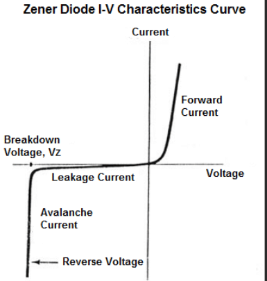
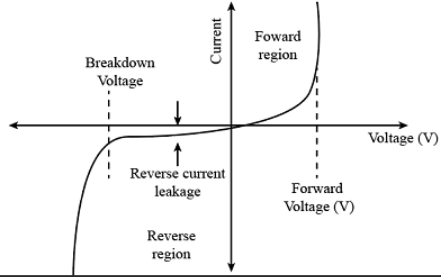
- A very small current, called the reverse saturation current or leakage current, flows due to the movement of minority charge carriers across the junction.
- The diode offers very high resistance in this state. This property of allowing current to flow in only one direction is called rectification.
Part 2: Full Wave Rectifier
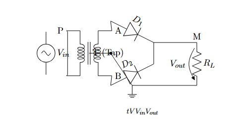
Step 1: Circuit Diagram:
A full-wave rectifier uses two diodes and a center-tapped transformer to convert both halves of an AC input into a pulsating DC output.

During the Positive Half-Cycle of AC Input:
- The upper end of the transformer secondary (A) is positive, and the lower end (B) is negative with respect to the center tap (T).
- Diode is connected to A, so it becomes forward-biased and conducts.
- Diode is connected to B, so it becomes reverse-biased and does not conduct.
- A current flows through diode and the load resistor in the direction from M to T.
During the Negative Half-Cycle of AC Input:
- The upper end (A) becomes negative, and the lower end (B) becomes positive with respect to the center tap (T).
- Diode is now reverse-biased and does not conduct.
- Diode is now forward-biased and conducts.
- A current flows through diode and the load resistor , again in the same direction from M to T.
Conclusion:
In both halves of the input AC cycle, the current flows through the load resistor in the same direction. This results in a unidirectional, pulsating DC voltage across the load. Since both halves of the AC wave are utilized, it is called a full-wave rectifier and is more efficient than a half-wave rectifier.
Official Solution
Official Solution
Step 2: When the same pure semiconductor is doped with a pentavalent impurity (such as phosphorus, arsenic, or antimony), each impurity atom forms covalent bonds with the silicon atoms and contributes an extra electron that is free to move within the crystal lattice. These free electrons act as negative charge carriers. The resulting material is called an n-type semiconductor, where electrons are the majority charge carriers.
Step 3: In both types of doping — p-type and n-type — the number of majority charge carriers (holes in p-type and electrons in n-type) increases significantly compared to the intrinsic (pure) semiconductor. As a result, the electrical conductivity of the semiconductor increases, making it more efficient for use in electronic components such as diodes, transistors, and integrated circuits.
Official Solution
Step 2: The color of the emitted light depends on the bandgap energy of the semiconductor material used in the LED. Different materials emit different wavelengths (colors) of light. For example:
Gallium arsenide (GaAs) emits infrared light,
Gallium phosphide (GaP) emits green or red light,
Gallium nitride (GaN) emits blue or white light.
By choosing appropriate semiconductor materials and doping levels, LEDs can be designed to emit a wide range of colors.
Step 3: LEDs are highly energy-efficient, converting most of the electrical energy into light with minimal heat loss. They also have a long operational life, are compact in size, and offer fast switching capabilities. Due to these advantages, LEDs are widely used in various applications such as display systems, indicator lights, lighting solutions, remote controls, and digital signage.
Official Solution
Official Solution
Official Solution
Official Solution
Official Solution
Step 2: The base-collector junction is reverse biased, creating a strong electric field that sweeps the injected carriers from the base into the collector region. Because the base is thin and lightly doped, most carriers pass through it without recombining.
Step 3: The small base current controls the large collector current, resulting in the amplification property of the transistor. This allows the transistor to act as a current amplifier, where a small input current at the base controls a much larger current flowing from emitter to collector.