Step 1: Define the Early Effect.
The Early effect, also known as base-width modulation, is the variation of the effective width of the base in a Bipolar Junction Transistor (BJT) due to a change in the collector-base junction voltage. This change in base width affects the collector current and the transistor's output characteristics. Step 2: Analyze the collector-base junction.
In the active region of operation, the collector-base junction is reverse-biased. This creates a depletion region at the junction. Step 3: Connect reverse bias to base width.
As the reverse bias voltage across the collector-base junction increases, the width of this depletion region increases. Since the depletion region extends into both the collector and the base, an increase in its width causes the effective (or neutral) width of the base region to decrease. This is the mechanism of the Early effect. Therefore, it is caused by the collector-base reverse bias.
02
PYQ 2025
medium
electronics-engineeringID: cuet-pg-
Negative feedback in amplifiersA. improves the signal-to-noise ratio at the input.B. improves the signal-to-noise ratio at the output.C. does not affect the signal-to-noise ratio at the output.D. reduces distortion.Choose the correct answer from the options given below:
1
A, C and D only
2
B, C and D only
3
A and C only
4
B and D only
Official Solution
Correct Option:
(1)
Negative feedback in amplifiers has the following effects:
A:Improves the signal-to-noise ratio at the input. This is generally true because negative feedback helps in reducing noise, thereby improving the input signal-to-noise ratio.
B:Improves the signal-to-noise ratio at the output. This statement is not true in all cases. Negative feedback can affect the output, but it doesn't necessarily improve the signal-to-noise ratio at the output.
C:Does not affect the signal-to-noise ratio at the output. Negative feedback primarily helps in reducing distortion and can make the signal-to-noise ratio at the output less sensitive to changes in the amplifier gain, but it doesn't significantly alter it.
D:Reduces distortion. Negative feedback is well known for reducing distortion by making the amplifier more linear.
Conclusion:
The correct answer is: A, C, and D only.
03
PYQ 2025
medium
electronics-engineeringID: cuet-pg-
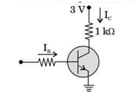
Assuming V and , the minimum base current ( ) required to drive the transistor in the figure to saturation is
1
56 A
2
140 A
3
60 A
4
4.3 A
Official Solution
Correct Option:
(1)
Step 1: Define the condition for saturation.
A BJT is in saturation when it is fully "on". In this state, the collector-emitter voltage drops to its minimum value, , and the collector current is limited primarily by the external circuit components. Step 2: Calculate the collector current at saturation ( ).
Using Kirchhoff's Voltage Law (KVL) on the collector-emitter loop:
At saturation, . So,
Substitute the given values:
Step 3: Calculate the minimum required base current ( ).
To ensure saturation, the base current must be large enough to support the saturation collector current. The relationship is given by the transistor's current gain, .
The minimum base current is the one that just puts the transistor at the edge of saturation:
Converting to microamperes: .
04
PYQ 2025
medium
electronics-engineeringID: cuet-pg-
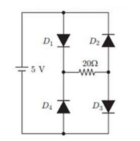
The circuit shown in the figure, the forward voltage of the diode is 0.7 V and its dynamic resistance is 2 . The current through the 20 resistor is
1
150 mA
2
200 mA
3
300 mA
4
400 mA
Official Solution
Correct Option:
(1)
Step 1: Analyze the circuit paths for the DC source.
The 5V source is connected to a diode bridge. The current will flow from the positive terminal and split. The 20 resistor is in one of the paths through the bridge. The path for current through the resistor is from the positive terminal of the source, through diode D1, through the 20 resistor, through diode D3, to the negative terminal of the source. Step 2: Apply Kirchhoff's Voltage Law (KVL) to the relevant loop.
The loop consists of the 5V source, diode D1, the 20 resistor, and diode D3.
Step 3: Model the forward-biased diodes.
The model for a forward-biased diode is a voltage source of 0.7V in series with its dynamic resistance of 2 .
So, and . Step 4: Solve for the current I.
Substitute the diode models into the KVL equation:
Convert the current to milliamperes: .
05
PYQ 2025
medium
electronics-engineeringID: cuet-pg-
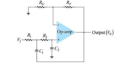
The circuit in the given figure is,
1
low-pass filter
2
high-pass filter
3
band-pass filter
4
band-reject filter
Official Solution
Correct Option:
(3)
Step 1: Analyze the circuit's behavior at very low frequencies ( ).
At DC or very low frequencies, capacitors act as open circuits.
Capacitor is in series with the input resistor . Since it's an open circuit, no input signal can reach the op-amp's inverting terminal. This means the output voltage will be zero. The gain is zero at low frequencies.
Step 2: Analyze the circuit's behavior at very high frequencies ( ).
At very high frequencies, capacitors act as short circuits.
Capacitor is in parallel with the feedback resistor . Acting as a short, it effectively shorts the feedback path, making the feedback impedance zero. In an inverting op-amp configuration, Gain . With , the gain of the circuit also approaches zero.
Step 3: Combine the low and high frequency analyses.
Since the circuit has zero gain at both very low and very high frequencies, but will have a non-zero gain at mid-frequencies (where the capacitors have finite reactance), it must be a band-pass filter. It passes a band of frequencies and rejects frequencies that are too low or too high.
06
PYQ 2025
medium
electronics-engineeringID: cuet-pg-
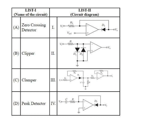
The circuit name (List-I) and their circuit diagram (List-II) are given in the table below. Match List-I with List-II.}
1
A - II, B - III, C - IV, D - I
2
A - III, B - II, C - I, D - IV
3
A - I, B - II, C - IV, D - III
4
A - II, B - I, C - IV, D - III
Official Solution
Correct Option:
(1)
In this problem, we are asked to match the circuit names from List-I with their corresponding diagrams in List-II. Let's analyze the circuits in List-I and compare them with the provided diagrams in List-II.
Analysis of Circuit Names (List-I):
A: This is a circuit name. After analyzing the diagrams, we see that this matches with diagram II in List-II.
B: This circuit name corresponds to diagram III in List-II based on its structure and components.
C: This circuit name corresponds to diagram IV in List-II, based on the specific components and configuration.
D: This circuit name corresponds to diagram I in List-II based on the matching components and structure.
Conclusion:
The correct matching is:
A - II, B - III, C - IV, D - I
07
PYQ 2025
medium
electronics-engineeringID: cuet-pg-
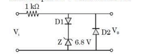
In the following limiter circuit, the input voltage is applied. Assume that the diode drop is 0.7 V when it is forward biased and the Zener breakdown voltage is 6.8 V. The maximum and minimum values of the output voltage, respectively, are
1
6.1 V, -0.7 V
2
0.7 V, -7.5 V
3
7.5 V, -0.7 V
4
7.5 V, -7.5 V
Official Solution
Correct Option:
(3)
Step 1: Analyze the circuit during the positive half-cycle of the input ( ).
During the positive half-cycle, current flows from the input through the 1 k resistor.
The lower diode D2 is reverse-biased and acts as an open circuit. In the upper branch, the conventional diode D1 is forward-biased, and the Zener diode Z is reverse-biased.
The upper branch will start to conduct and clamp the output voltage when the voltage across it is sufficient to forward bias D1 and cause the Zener to enter breakdown. The output voltage will be limited to:
Step 2: Analyze the circuit during the negative half-cycle of the input ( ).
During the negative half-cycle, the voltage becomes negative.
In the upper branch, the conventional diode D1 is reverse-biased, acting as an open circuit. This entire branch is non-conducting. The lower diode D2 is forward-biased.
The output voltage will be clamped by the forward-biased diode D2. The minimum output voltage will be:
Thus, the output voltage is clipped at +7.5 V and -0.7 V.
08
PYQ 2025
medium
electronics-engineeringID: cuet-pg-
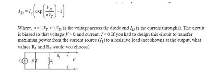
Consider the diode circuit shown below. The diode, D, obeys the current-voltage characteristic . The circuit is biased so that voltage and current . If you had to design this circuit to transfer maximum power from the current source ( ) to a resistive load (not shown) at the output, what values for R1 and R2 would you choose?A. Small , B. Large , C. Small , D. Large .Choose the correct answer from the options given below:
1
A and C
2
B and C
3
A and D
4
B and D
Official Solution
Correct Option:
(4)
Step 1: Understand the goal.
The objective is to transfer the maximum possible power from the current source to an external load resistor connected at the output terminals (where V and I are measured). This is a problem of maximizing power delivery efficiency. Step 2: Analyze the current paths.
The current from the source flows into the central node. From there, it splits into several paths:
Through the diode (current ). Through resistor (current ). Through resistor (current ). To the external load (current ).
According to KCL, . Step 3: Identify power losses.
The power generated by the source is distributed among all the components. The power delivered to the load is . The power lost or consumed by the internal components is . To maximize , we must minimize . Step 4: Determine how to minimize losses in R1 and R2.
The power dissipated in the resistors is and . To minimize this power dissipation, the currents and must be minimized. This means that the resistances and should be as large as possible. Large values of and create high impedance paths that prevent the source current from being shunted away from the load. Step 5: Conclude the design choice.
To maximize the current (and thus power) delivered to the external load, the shunt paths through and must have very high resistance. Therefore, we should choose a large and a large . This corresponds to options B and D.
09
PYQ 2025
medium
electronics-engineeringID: cuet-pg-
Crossover distortion behavior is characteristic of
1
Class A amplifier.
2
Class B amplifier.
3
Class AB amplifier.
4
Common-base amplifier.
Official Solution
Correct Option:
(2)
Step 1: Define Crossover Distortion.
Crossover distortion is a type of distortion that occurs in push-pull amplifiers. It is the distortion that happens during the transition, or "crossover," when one transistor in the push-pull pair turns off and the other turns on. Step 2: Analyze Class B Amplifier operation.
A Class B amplifier uses two complementary transistors (e.g., NPN and PNP) where each transistor conducts for only one-half (180 degrees) of the input signal cycle. For a silicon BJT, a base-emitter voltage of about 0.7V is required for the transistor to start conducting. Step 3: Identify the cause of distortion.
When the input signal is near zero volts (crossing over from positive to negative or vice-versa), neither transistor is conducting because the input voltage is insufficient (less than 0.7V) to turn either one on. This creates a "dead zone" in the output signal around the zero-crossing point, which is known as crossover distortion. Class AB amplifiers are designed specifically to eliminate this by providing a small quiescent bias current that keeps both transistors slightly on even with no signal.
About Analog Electronics - CUET-PG
Analog Electronics is a vital chapter for CUET-PG aspirants. Mastering the concepts covered in this chapter is essential for securing a top rank.
By rigorously practicing the previous year questions associated with this chapter, you can identify high-yield topics, understand the examiner's perspective, and boost your confidence during the actual exam.
Frequently Asked Questions
Why focus on Analog Electronics PYQs?
Analyzing PYQs for this specific chapter reveals the most frequently tested concepts and the typical complexity of questions, allowing you to tailor your study plan efficiently.
How to best use this analysis?
Review the topic breakdown to see which sub-topics within Analog Electronics carry the most weight. Then, tackle the questions iteratively to solidify your understanding.