Analog Electronics
10 previous year questions.
High-Yield Trend
Chapter Questions 10 MCQs
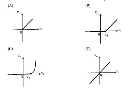
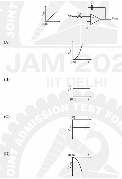
Which one of the following graphs shows the correct variation of with ? Here, is the voltage drop across the diode and the Op-Amp is assumed to be ideal. 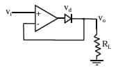
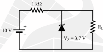
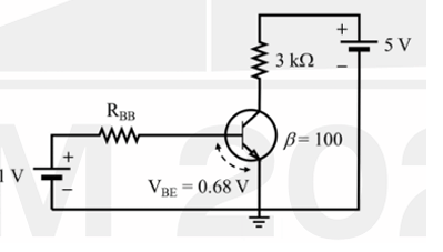
For the following circuit, the collector voltage with respect to ground will be .............. V. (Emitter diode voltage is 0.7 V and of the transistor is large.) (Specify your answer in volts up to one digit after the decimal point.) 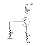
For the given circuit, the value of base current of the npn transistor is ........... mA. ( is the current gain and assume the Op-Amp as ideal.) (Specify your answer in mA up to two digits after decimal.) 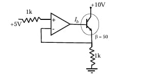
In the following circuit, is much larger than the input period. Assume diode is ideal and is large. The dc output voltage across will be .............. V. (Specify answer up to one digit after the decimal point.) 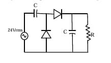
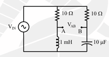
For the AC circuit shown in the figure, and , the phase difference between and is at the input signal frequency of ............. kHz. (Round off to 2 decimal places) 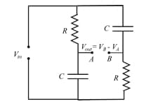
In the circuit shown in the figure, both OPAMPs are ideal. The output for the circuit is: 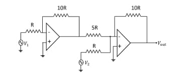
About Analog Electronics - IIT-JAM-PH
Analog Electronics is a vital chapter for IIT-JAM-PH aspirants. Mastering the concepts covered in this chapter is essential for securing a top rank.
By rigorously practicing the previous year questions associated with this chapter, you can identify high-yield topics, understand the examiner's perspective, and boost your confidence during the actual exam.
Frequently Asked Questions
Why focus on Analog Electronics PYQs?
Analyzing PYQs for this specific chapter reveals the most frequently tested concepts and the typical complexity of questions, allowing you to tailor your study plan efficiently.
How to best use this analysis?
Review the topic breakdown to see which sub-topics within Analog Electronics carry the most weight. Then, tackle the questions iteratively to solidify your understanding.