IIT-JAM-PH SERIES
Physics

Solid State Physics Devices Electronics

25 previous year questions.

Volume: 25 Ques
Yield: High

High-Yield Trend

6
2025
8
2024
1
2023
4
2022
3
2020
3
2018

Chapter Questions
25 MCQs

01
PYQ 2018
medium
physics ID: iit-jam-

For a metal, electron density is . The Fermi energy is ................. eV. (Specify answer up to one digit after the decimal point.)

02
PYQ 2018
medium
physics ID: iit-jam-
In a pn junction, dopant concentration on p-side is higher than n-side. Which statements are correct when the junction is unbiased?
1
The width of the depletion layer is larger on the n-side.
2
Fermi energy is higher on the p-side.
3
Negative charge per unit area on p-side equals positive charge per unit area on n-side.
4
Built-in potential depends on dopant concentration.
03
PYQ 2018
medium
physics ID: iit-jam-
Which of the combinations of crystal structure and coordination number is correct?
1
body-centered cubic – 8
2
face-centered cubic – 6
3
diamond – 4
4
hexagonal closed packed – 12
04
PYQ 2020
medium
physics ID: iit-jam-

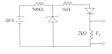
The figure shows a circuit containing two diodes and with threshold voltages of 0.7 V and 0.3 V, respectively. Considering the simplified diode model, which assumes diode I–V characteristics as shown in the plot on the right, the current through the resistor is ......... µA.

05
PYQ 2020
medium
physics ID: iit-jam-

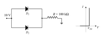
In the transistor circuit given in the figure, the emitter-base junction has a voltage drop of 0.7 V. A collector-emitter voltage of 14 V reverse biases the collector. Assuming the collector current to be the same as the emitter current, the value of is ........... k .

06
PYQ 2020
medium
physics ID: iit-jam-

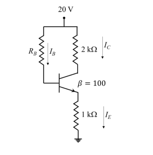
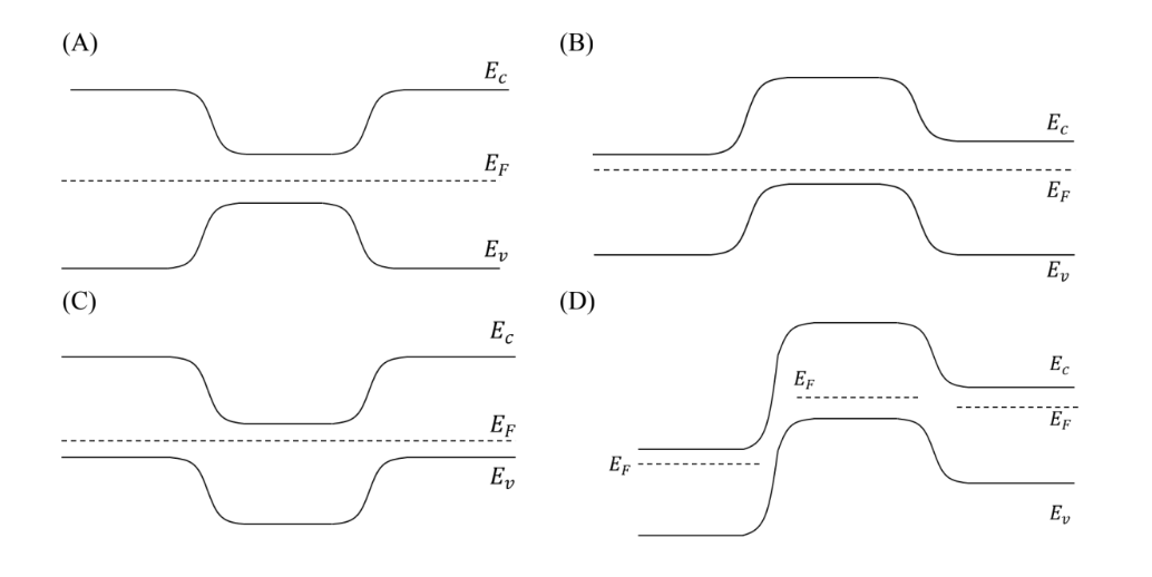
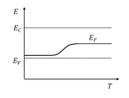
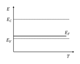
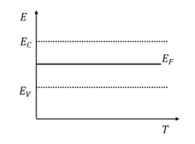
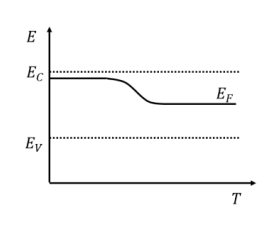
For an unbiased Silicon transistor in thermal equilibrium, which one of the following electronic energy band diagrams is correct? ( = conduction band minimum, = valence band maximum, = Fermi level.)


1
(A)
2
(B)
3
(C)
4
(D)
07
PYQ 2022
medium
physics ID: iit-jam-
For an ideal intrinsic semiconductor, the Fermi energy at 0 K
1
lies at the top of the valence band
2
lies at the bottom of the conduction band
3
lies at the center of the bandgap
4
lies midway between center of the bandgap and bottom of the conduction band
08
PYQ 2022
hard
physics ID: iit-jam-
For the given circuit, R = 125 Ω, RL = 470 Ω, Vz = 9V, and = 65 mA. The minimum and maximum values of the input voltage ( ) for which the Zener diode will be in the 'ON' state are
For the given circuit, R = 125 Ω, RL = 470 Ω, Vz = 9V
1
Vimin = 9.0 V and Vimax = 11.4 V
2
Vimin = 9.0 V and Vimax = 19.5 V
3
Vimin = 11.4 V and Vimax = 15.5 V
4
Vimin = 11.4 V and Vimax = 19.5 V
09
PYQ 2022
easy
physics ID: iit-jam-
For an n-type silicon, an extrinsic semiconductor, the natural logarithm of normalized conductivity (σ) is plotted as a function of inverse temperature. Temperature interval-I corresponds to the intrinsic regime, interval-II corresponds to saturation regime and interval-III corresponds to the freeze-out regime, respectively. Then
an n-type silicon, an extrinsic semiconductor
1
the magnitude of the slope of the curve in the temperature interval-I is proportional to the bandgap, Eg
2
the magnitude of the slope of the curve in the temperature interval-III is proportional to the ionization energy of the donor, Ed
3
in the temperature interval-II, the carrier density in the conduction band is equal to the density of donors
4
in the temperature interval-III, all the donor levels are ionized
10
PYQ 2022
hard
physics ID: iit-jam-
For the given operational amplifier circuit R1 = 120 Ω, R2 = 1.5 k and Vs = 0.6 V, then the output current I0 is ____mA.
the given operational amplifier circuit R1=120Ω, R2=1.5k
11
PYQ 2023
medium
physics ID: iit-jam-
In an extrinsic p-type semiconductor, which of the following schematic diagram depicts the variation of the Fermi energy level (EF) with temperature (T) ?
1
schematic diagram 1
2
Schematic Diagram 2
3
Schematic Diagram 3
4
Schematic Diagram 4
12
PYQ 2024
medium
physics ID: iit-jam-
A Zener diode (rating 10V, 2W) and a normal diode (turn-on voltage 0.7V) are connected in a circuit as shown in the figure. The voltage drop 𝑉𝐿 across the 2kΩ resistance is ____V. (Rounded off to one decimal place)
A Zener diode and a normal diode
13
PYQ 2024
medium
physics ID: iit-jam-
A charge of −9C is placed at the center of a concentric spherical shell made of a linear dielectric material (relative permittivity 9) and having inner and outer radii of 0.1m and 0.2m, respectively. The total charge induced on its inner surface is ______C. (Rounded off to two decimal place)
14
PYQ 2024
easy
physics ID: iit-jam-
Consider a p-n junction diode which has 1023 acceptor-atoms/m3 in the p-side and 1022 donor-atoms/m3 in the n-side. If the depletion width in the p-side is 0.16µm, then the value of depletion width in the n-side will be ______µm. (Rounded off to one decimal place)
15
PYQ 2024
medium
physics ID: iit-jam-
For the LCR AC-circuit (resonance frequency ωo) shown in the figure below, choose the correct statement(s).
the LCR AC-circuit
1
ωo depends on the values of L, C, and R
2
At ω= ωo, voltage VR and current I are in-phase
3
The amplitude of VR at ω=ωo/2 is independent of R
4
The amplitude of VR at ω= ωo is independent of L and C
16
PYQ 2024
medium
physics ID: iit-jam-
A pure Si crystal can be converted to an n-type crystal by doping with
1
P
2
As
3
Sb
4
In
17
PYQ 2024
easy
physics ID: iit-jam-
In the following OP-AMP circuit, 𝑣𝑖𝑛 and 𝑣𝑜𝑢𝑡 represent the input and output signals, respectively.
OP-AMP circuit
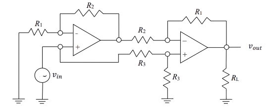
Choose the correct statement(s):
1
𝑣𝑜𝑢𝑡 is out-of-phase with 𝑣𝑖𝑛
2
Gain is unity when R1 = R2
3
𝑣𝑜𝑢𝑡 is in-phase with 𝑣𝑖n
4
𝑣𝑜𝑢𝑡 is zero
18
PYQ 2024
hard
physics ID: iit-jam-
A transistor (β=100, 𝑉𝐵𝐸 = 0.7𝑉) is connected as shown in the circuit below.
circuit-A transistor
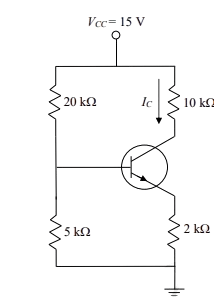
The current IC will be mA. (Rounded off to two decimal places)
19
PYQ 2024
medium
physics ID: iit-jam-
Consider the following logic circuit.
logic circuit.
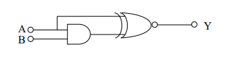
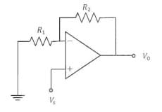
The output Y is LOW when:
1
A is HIGH and B is LOW
2
A is LOW and B is HIGH
3
Both A and B are LOW
4
Both A and B are HIGH
20
PYQ 2025
medium
physics ID: iit-jam-
The ratio of the density of atoms between the (111) and (110) planes in a simple cubic (sc) lattice is ____. (up to two decimal places)
21
PYQ 2025
medium
physics ID: iit-jam-
The packing fraction for a two-dimensional hexagonal lattice having sides 2r with atoms of radii r placed at each vertex and at the center is _____. (up to two decimal places)
22
PYQ 2025
medium
physics ID: iit-jam-
In an orthorhombic crystal, the lattice constants are 3.0 \AA, 3.2 \AA, and 4.0 \AA. The distance between the successive (101) planes is \rule{1cm{0.15mm} \AA. (up to one decimal place)}
23
PYQ 2025
medium
physics ID: iit-jam-
An ideal p-n junction diode (ideality factor ) is operating in forward bias at room temperature (thermal energy = 26 meV). If the diode current is 26 mA for an applied bias of 1.0 V, the dynamic resistance ( ) is \rule{1cm{0.15mm} . (up to two decimal places)}
24
PYQ 2025
medium
physics ID: iit-jam-
For a body centered cubic (bcc) system, the x-ray diffraction peaks are observed for the following value(s)
1
3
2
4
3
5
4
7
25
PYQ 2025
medium
physics ID: iit-jam-
Which of these cubic lattice plane pairs is(are) perpendicular to each other?
1
(100), (010)
2
(220), (001)
3
(110), (010)
4
(112), (220)