UP-BOARD-XII SERIES Physics
Pn Junction Diode
19 previous year questions.
Volume: 19 Ques
Yield: Medium
High-Yield Trend
16
2025 3
2024 Chapter Questions 19 MCQs
01
PYQ 2024
medium
physics ID: up-board
There is minimum deviation of light ray on passing through a prism (n = ). If the angle of incidence is twice the angle of refraction for this ray, then what will be the angle of prism and the angle of refraction?
02
PYQ 2024
medium
physics ID: up-board
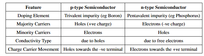
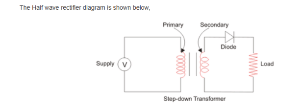
Compare features of p-type and n-type semiconductors. Draw circuit diagram of half-wave rectifier of p-n junction diode and explain it.
03
PYQ 2024
medium
physics ID: up-board
Explain the operation of p-n junction diode in forward bias.
04
PYQ 2025
easy
physics ID: up-board
Resistance of an ideal p-n junction diode in reverse bias is:
1
zero
2
infinite
3
in between zero and infinite
4
none of these
05
PYQ 2025
medium
physics ID: up-board
Find current through the battery in the circuit shown in fig :
\includegraphics[width=0.5\linewidth]{1.png}
06
PYQ 2025
medium
physics ID: up-board
Explain the working of a forward biased ( ) junction diode by making circuit diagram and by drawing its characteristic graph. Define its dynamic resistance.
07
PYQ 2025
medium
physics ID: up-board
Explain the working method of p-n junction diode in reverse bias with the help of a circuit diagram.
08
PYQ 2025
medium
physics ID: up-board
Explain the meaning of rectification. Using a p-n junction diode, draw a circuit diagram of a full-wave rectifier and give a brief description of its working. Give a graphical representation of input and output voltage/current.
09
PYQ 2025
medium
physics ID: up-board
Draw a circuit diagram to obtain characteristic curve in forward bias of p-n junction diode. Mention the effect of forward bias on depletion layer of the junction.
10
PYQ 2025
medium
physics ID: up-board
Explain the working method of a reverse biased (p-n) junction diode by making its circuit diagram and explain avalanche breakdown with the help of its V-I characteristic graph.
11
PYQ 2025
medium
physics ID: up-board
What is the rectifying process? Explain the half-wave rectifying action of a (p-n) junction diode with the help of a circuit diagram.
12
PYQ 2025
medium
physics ID: up-board
An a.c. voltage of peak value 20 V is connected in series with a silicon diode and a load resistance of 500 . The forward resistance of the diode is 10 and the resistive voltage is 0.7 V. Find the peak current through the diode and peak voltage across the load.
13
PYQ 2025
medium
physics ID: up-board
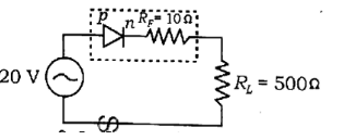
On the basis of energy band diagram in solids, explain the difference between conductor, semiconductor, and insulator. What is the need of doping in pure semiconductors? Write the value of current in the ideal diodes and in the given circuit.
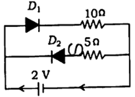
14
PYQ 2025
medium
physics ID: up-board
Explain the working method of a reverse biased (p-n) junction diode by making its circuit diagram and explain avalanche breakdown with the help of its V-I characteristic graph.
15
PYQ 2025
medium
physics ID: up-board
What is the rectifying process? Explain the half-wave rectifying action of a (p-n) junction diode with the help of a circuit diagram.
16
PYQ 2025
medium
physics ID: up-board
Explain the working method of p-n junction diode in reverse bias with the help of a circuit diagram.
17
PYQ 2025
medium
physics ID: up-board
Resistance of an ideal p-n junction diode in reverse bias is:
1
zero
2
infinite
3
in between zero and infinite
4
none of these
18
PYQ 2025
medium
physics ID: up-board
The resistance of p-n junction diode in forward bias is 25 ohm. How much voltage in forward bias be changed so that the change in current would be 2 mA?
19
PYQ 2025
medium
physics ID: up-board
Explain the working of a forward biased ( ) junction diode by making circuit diagram and by drawing its characteristic graph. Define its dynamic resistance.

