What are doped semiconductors? Explain the effect of (i) doping and (ii) temperature on the conductivity of semiconductors.
Official Solution
Correct Option:
(1)
Step 1: Definition. Pure semiconductors (Si, Ge) have limited conductivity. When a small quantity of impurity is added, they become doped semiconductors (extrinsic type). Step 2: Effect of doping. - Doping with pentavalent impurities (P, As) gives N-type semiconductor (extra electrons as majority carriers). - Doping with trivalent impurities (B, Al) gives P-type semiconductor (holes as majority carriers). - Conductivity increases drastically because of increased number of charge carriers. Step 3: Effect of temperature. - As temperature rises, more covalent bonds break, releasing additional charge carriers. - Hence conductivity increases with temperature (unlike metals where resistance increases). Step 4: Conclusion. Thus, doping and increase in temperature both increase the conductivity of semiconductors.
02
PYQ 2023
medium
physicsID: up-board
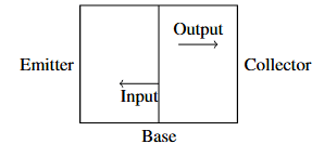
Explain the working process of the amplifying action of an n-p-n transistor in common emitter configuration by making a circuit diagram and obtain the formula for voltage amplification.
Official Solution
Correct Option:
(1)
Step 1: Basic Structure of an n-p-n Transistor. An n-p-n transistor consists of three layers of semiconductor material: the emitter (n-type), base (p-type), and collector (n-type). In a common emitter configuration, the emitter is common to both the input and output circuits. Step 2: Circuit Diagram. Here’s the circuit diagram for the common emitter amplifier:
Step 3: Working of the Amplifying Action. In the common emitter configuration, the input signal is applied to the base-emitter junction, and the output is taken across the collector-emitter junction. When a small input voltage is applied to the base, it causes a small change in the base current . This small change causes a much larger change in the collector current , because the current gain of the transistor is typically large. The output voltage is therefore amplified in proportion to the input voltage. Step 4: Voltage Amplification Formula. The voltage gain of the amplifier is the ratio of the change in the output voltage to the change in the input voltage:
For a common emitter amplifier, the voltage gain is approximately:
where:
- is the collector resistance,
- is the small-signal emitter resistance. Step 5: Conclusion. Thus, the n-p-n transistor in common emitter configuration amplifies the input voltage by a factor of , and the amplification depends on the ratio of the collector resistance to the small-signal emitter resistance.
03
PYQ 2023
medium
physicsID: up-board
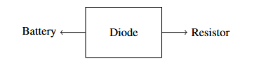
Explain the working process of a forward biased p-n junction diode with the help of a circuit diagram. Show the dynamic resistance by making a graph between the forward voltage and forward current.
Official Solution
Correct Option:
(1)
Step 1: Working of a Forward Biased p-n Junction Diode. In a forward biased p-n junction diode, the positive terminal of the battery is connected to the p-type material, and the negative terminal is connected to the n-type material. This reduces the width of the depletion region and allows current to flow through the diode once the forward voltage exceeds the threshold (or "cut-in" voltage). Step 2: Circuit Diagram. Here is the circuit diagram of a forward biased p-n junction diode:
Step 3: Dynamic Resistance. The dynamic resistance of the diode is defined as the change in voltage divided by the corresponding change in current :
Step 4: Graph Between Forward Voltage and Forward Current. The current through a forward biased p-n junction diode increases exponentially with the applied forward voltage after the threshold voltage. The relationship between the forward voltage and the forward current is given by the Shockley diode equation:
where is the saturation current, is the ideality factor, and is the thermal voltage. Step 5: Conclusion. Thus, as the forward voltage increases, the current increases exponentially. The dynamic resistance decreases as the current increases, and the diode exhibits a nonlinear I-V characteristic.
04
PYQ 2023
medium
physicsID: up-board
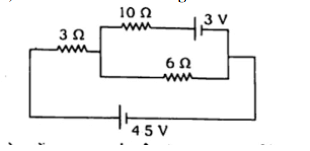
Find the current through the 10Ω resistor shown in the figure.
Official Solution
Correct Option:
(1)
Step 1: Apply Kirchhoff’s Rules. We are given a circuit with resistors of , , and , and a voltage source of and . We will apply Kirchhoff’s Voltage Law (KVL) to the loop and solve for the current using Ohm’s Law:
Where and .
After solving the equation, we get:
Final Answer:
The current through the 10Ω resistor is .
05
PYQ 2023
medium
physicsID: up-board
N-type semi-conductor is:
1
Negatively charged
2
Positively charged
3
Electrically neutral
4
None of these
Official Solution
Correct Option:
(3)
Step 1: Nature of N-type semiconductor. In N-type semiconductors, electrons are majority carriers. But for every extra electron, there is a positive ion core. Step 2: Neutrality. The number of positive and negative charges balance each other. Step 3: Conclusion. Hence, N-type semiconductors are overall electrically neutral.
About Semiconductors - UP-BOARD-XII
Semiconductors is a vital chapter for UP-BOARD-XII aspirants. Mastering the concepts covered in this chapter is essential for securing a top rank.
By rigorously practicing the previous year questions associated with this chapter, you can identify high-yield topics, understand the examiner's perspective, and boost your confidence during the actual exam.
Frequently Asked Questions
Why focus on Semiconductors PYQs?
Analyzing PYQs for this specific chapter reveals the most frequently tested concepts and the typical complexity of questions, allowing you to tailor your study plan efficiently.
How to best use this analysis?
Review the topic breakdown to see which sub-topics within Semiconductors carry the most weight. Then, tackle the questions iteratively to solidify your understanding.