Applications Of Pn Junction
High-Yield Trend
Questions 17 MCQs
A common emitter amplifier has a voltage gain of 50, an input impedance of 100Ω, and an output impedance of 200Ω. The power gain of the amplifier is:
1. 500
2. 1000
3. 1250
4. 100
The voltage gain of an amplifier with 9% negative feedback is 10. The voltage gain without feedback will be:
1. 90
2. 10
3. 1.25
4. 100
The device that can act as a complete electronic circuit is:
1. Junction diode
2. Integrated circuit
3. Junction transistor
4. Zener diode
A common emitter amplifier has a voltage gain of 50, an input impedance of 100 Ω and an output impedance of 200 Ω. The power gain of the amplifier is:
1. 500
2. 1000
3. 1250
4. 50
A transistor is operated in a common emitter configuration at Vc =2 V such that a change in the base current from 100 to 300 produces a change in the collector current from 10 mA to 20mA. The current gain is:
1. 75
2. 100
3. 25
4. 50
In a CE transistor amplifier, the audio signal voltage across the resistance of 2 k is 2V. If the base resistance is 1 k and the current amplification of the transistor is 100, the input signal voltage is:
1. 0.1 V
2. 1.0 V
3. 1 mV
4. 10 mV
Transfer characteristics [output voltage () vs input voltage ()] for a base biased transistor in CE configurations are as shown in the figure. For using the transistor as a switch, it is used:
1. In region III
2. Both in the region (I) and (III)
3. In region II
4. In region I
The input signal given to a CE amplifier having a voltage gain of 150 is . The corresponding output signal will be:
1.
2.
3.
4.
For the CE transistor amplifier, the audio signal voltage across the collector resistance of 2k is 4V. If the current amplification factor of the transistor is 100 and the base resistance is 1k, then the input signal voltage is:
1. 10 mV
2. 20 mV
3. 30 mV
4. 15 mV
In a common-emitter transistor amplifier, the audio signal voltage across the collector is 3V. The resistance of the collector is 3k. If the current gain is 100 and the base resistance is 2k, the voltage and power gain of the amplifier are:
1. 15 and 200
2. 150 and 15000
3. 20 and 2000
4. 200 and 1000
In the circuit shown in the figure, the input voltage Vi is 20 V, VBE = 0, and VCE = 0. The values of IB, IC and are given by:
1.
2.
3.
4.
An n-p-n transistor is connected in a common emitter configuration (see figure) in which collector voltage drop across load resistance ( 800 ) connected to the collector circuit is 0.8 V. The collector current is:
1. 2 mA
2. 0.1 mA
3. 1 mA
4. 0.2 mA
| Statement A: | A Zener diode is connected in reverse bias when used as a voltage regulator. |
| Statement B: | The potential barrier of junction lies between V to V. |
| 1. | Statement A is correct and Statement B is incorrect. |
| 2. | Statement A is incorrect and Statement B is correct. |
| 3. | Statement A and Statement B both are correct. |
| 4. | Statement A and Statement B both are incorrect. |
| Statement I: | Photovoltaic devices can convert optical radiation into electricity. |
| Statement II: | The Zener diode is designed to operate under reverse bias in the breakdown. |
| 1. | Statement I is incorrect but Statement II is correct. |
| 2. | Both Statement I and Statement II are correct. |
| 3. | Both Statement I and Statement II are incorrect. |
| 4. | Statement I is correct but Statement II is incorrect. |
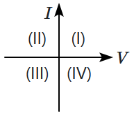
| A. | For a solar-cell, the characteristics lies in the IV quadrant of the given graph. |
| B. | In a reverse-biased pn junction diode, the current measured in ( ), is due to majority charge carriers. |
| 1. | A is incorrect but B is correct. |
| 2. | Both A and B are correct. |
| 3. | Both A and B are incorrect. |
| 4. | A is correct but B is incorrect. |
Preparing Applications Of Pn Junction for NEET
Applications Of Pn Junction is a specific sub-topic that frequently appears in the NEET examination. Understanding the underlying principles and practicing targeted questions is key to mastering this concept.
The questions compiled above are previous year questions (PYQs) directly related to Applications Of Pn Junction. Practicing these specific questions helps you understand the difficulty level and the examiner's approach to this topic.
Topic Frequently Asked Questions
Is Applications Of Pn Junction a high-weightage topic?
You can refer to the priority and consistency badges at the top of this page. High priority topics should be thoroughly revised multiple times before the exam.
Should I memorize the solutions?
No, it is highly recommended to understand the core concept and methodology behind each solution rather than memorizing them, as exact questions are rarely repeated, but the concepts definitely are.