Logic Gates
High-Yield Trend
Questions 19 MCQs
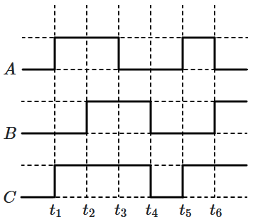
The following figure shows a logic gate circuit with two inputs A and B and the output C. The voltage waveforms of A, B, and C are as shown below:
The logic circuit gate is:
1. AND gate
2. NAND gate
3. NOR gate
4. OR gate
In the following circuit, the output for all possible inputs and is expressed by the truth table:
| 1. | A | B | Y | 2. | A | B | Y |
| 0 | 0 | 0 | 0 | 0 | 1 | ||
| 0 | 1 | 0 | 0 | 1 | 1 | ||
| 1 | 0 | 0 | 1 | 0 | 1 | ||
| 1 | 1 | 1 | 1 | 1 | 0 | ||
| 3. | 0 | 0 | 1 | 4. | 0 | 0 | 0 |
| 0 | 1 | 0 | 0 | 1 | 1 | ||
| 1 | 0 | 0 | 1 | 0 | 1 | ||
| 1 | 1 | 1 | 1 | 1 | 1 |
The circuit is equivalent to:
1. AND gate
2. NAND gate
3. NOR gate
4. OR gate
The symbolic representation of four logic gates is as shown:
| (i) | (ii) | ||
| (ii) | (iv) |
The logic symbols for OR, NOT, and NAND gates are respectively:
1. (iii), (iv), (ii)
2. (iv), (i), (iii)
3. (iv), (ii), (i)
4. (i), (iii), (iv)
To get an output Y = 1 from the circuit shown below, the input must be:
1. A=0 B=1 C=0
2. A=0 B=0 C=1
3. A=1 B=0 C=1
4. A=1 B=0 C=0
The symbolic representation of four gates is shown as:
Pick out which ones are for AND, NAND, and NOT gates, respectively.
1. (i), (iv), and (iii)
2. (ii), (iii), and (iv)
3. (ii), (iv), and (iii)
4. (ii), (iv), and (i)
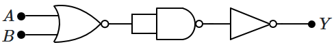
The figure shows a logic circuit with two inputs and and the output . The voltage waveforms across , , and are as given. The logic circuit gate is:
1. gate
2. gate
3. gate
4. gate
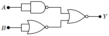
The output of the logic circuit shown in the figure will be:
1.
2.
3.
4. None of the above
What is the output in the following circuit, when all the three inputs , , and are first and then ?
1.
2.
3.
4.
The given electrical network is equivalent to:
| 1. | gate | 2. | gate |
| 3. | gate | 4. | gate |
In the combination of the following gates, the output can be written in terms of inputs and as:
1.
2.
3.
4.
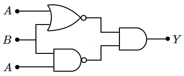
The correct Boolean operation represented by the circuit diagram given above is:
1.
2.
3.
4.
Which of the following gate is called the universal gate?
1. gate
2. gate
3. gate
4. gate
For the given circuit, the input digital signals are applied at the terminals , and . What would be the output at terminal ?
| 1. | |
| 2. | |
| 3. | |
| 4. |
| 1. |
|
|||||||||||||||
| 2. |
|
|||||||||||||||
| 3. |
|
|||||||||||||||
| 4. |
|
| 1. |
|
|||||||||||||||
| 2. |
|
|||||||||||||||
| 3. |
|
|||||||||||||||
| 4. |
|
| 0 0 1 1 | 0 1 0 1 | 1 0 1 0 |
1.
2.
3.
4.
| 1. | gate | 2. | gate |
| 3. | gate | 4. | gate |
| 1. | OR | 2. | NOR |
| 3. | AND | 4. | NAND |
Preparing Logic Gates for NEET
Logic Gates is a specific sub-topic that frequently appears in the NEET examination. Understanding the underlying principles and practicing targeted questions is key to mastering this concept.
The questions compiled above are previous year questions (PYQs) directly related to Logic Gates. Practicing these specific questions helps you understand the difficulty level and the examiner's approach to this topic.
Topic Frequently Asked Questions
Is Logic Gates a high-weightage topic?
You can refer to the priority and consistency badges at the top of this page. High priority topics should be thoroughly revised multiple times before the exam.
Should I memorize the solutions?
No, it is highly recommended to understand the core concept and methodology behind each solution rather than memorizing them, as exact questions are rarely repeated, but the concepts definitely are.