When the conductivity of a semiconductor is due only to the breaking up of the covalent bonds, the semiconductor is known as:
1
Donor
2
Extrinsic
3
Intrinsic
4
Acceptor
Official Solution
Correct Option:
(3)
Step 1: Define intrinsic semiconductors. In intrinsic semiconductors, the conductivity is due to the breaking of covalent bonds, creating free electrons and holes. Step 2: Conclusion. Thus, when conductivity is due to the breaking up of covalent bonds, the semiconductor is intrinsic.
02
PYQ 2006
medium
physicsID: viteee-2
In a P-type semiconductor, the acceptor impurity is:
1
Just above the valence band
2
Just below the conduction band
3
Just above the conduction band
4
Just below the valence band
Official Solution
Correct Option:
(4)
Step 1: P-type semiconductor characteristics. In a P-type semiconductor, the acceptor impurities are atoms with one less electron than the semiconductor atoms, and they create holes just below the valence band. Step 2: Conclusion. Thus, in a P-type semiconductor, the acceptor impurity is located just below the valence band.
03
PYQ 2007
medium
physicsID: viteee-2
Identify the logic gate from the following TRUTH table
1
NOR gate
2
AND gate
3
NOT gate
4
NAND gate
Official Solution
Correct Option:
(1)
Step 1: Analyzing the truth table. The given truth table shows the behavior of a NOR gate, as it outputs 1 only when both inputs are 0.
Step 2: Conclusion. Thus, the correct answer is option (A).
Final Answer:
04
PYQ 2007
medium
physicsID: viteee-2
In Boolean algebra, is equal to
1
2
3
4
Official Solution
Correct Option:
(4)
Step 1: Boolean identity. In Boolean algebra, represents the AND operation, while the options provided represent different logical expressions.
Step 2: Conclusion. The correct answer is option (D).
Final Answer:
05
PYQ 2007
medium
physicsID: viteee-2
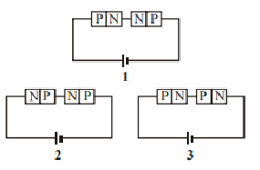
Two identical P-N junctions are connected in series in three different ways as shown below to a battery. The potential drop across the P-N junctions are equal in
1
circuits 2 and 3
2
circuits 1 and 2
3
circuits 1 and 3
4
none of the circuit
Official Solution
Correct Option:
(1)
Step 1: Analyzing the circuits. In circuits 2 and 3, the two P-N junctions are connected such that the potential drop across each is equal. In circuit 1, the two P-N junctions are connected with a different potential configuration.
Step 2: Conclusion. Therefore, the correct answer is option (A).
Final Answer:
06
PYQ 2007
medium
physicsID: viteee-2
The temperature coefficient of a zener mechanism is
1
negative
2
positive
3
infinity
4
zero
Official Solution
Correct Option:
(1)
Step 1: Zener Diode Characteristics. Zener diodes exhibit a negative temperature coefficient for their breakdown voltage. As the temperature increases, the breakdown voltage decreases.
Step 2: Conclusion. Therefore, the correct answer is option (A).
Final Answer:
07
PYQ 2007
medium
physicsID: viteee-2
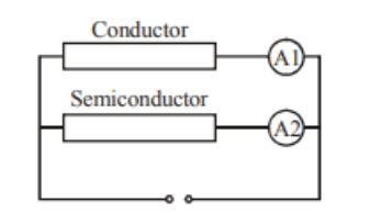
A conductor and a semi-conductor are connected in parallel as shown in the figure. At a certain voltage both ammeters register the same current. If the voltage of the DC source is increased then
1
the ammeter connected to the semiconductor will register higher current than the ammeter connected to the conductor
2
the ammeter connected to the conductor will register higher current than the ammeter connected to the semiconductor
3
the ammeters connected to both semiconductor and conductor will register the same current
4
the ammeter connected to both semiconductor and conductor will register no change in the current
Official Solution
Correct Option:
(3)
Step 1: Current through the components. When the conductor and semiconductor are in parallel, the current through each depends on the resistance of the material. When the voltage is increased, the current will increase, but the ratio of currents remains the same.
Step 2: Conclusion. Thus, the correct answer is option (C).
Final Answer:
08
PYQ 2008
medium
physicsID: viteee-2
The reverse saturation current of p--n diode
1
depends on doping concentrations
2
depends on diffusion lengths of carriers
3
depends on the doping concentrations and diffusion lengths
4
depends on the doping concentrations, diffusion length and device temperature
Official Solution
Correct Option:
(4)
Step 1: Recall expression of reverse saturation current. Reverse saturation current is mainly due to minority carriers:
Step 2: Identify dependencies. From this expression, depends on: (i) doping concentrations (ii) diffusion constants (iii) diffusion lengths (iv) intrinsic concentration Step 3: Role of temperature. strongly increases with temperature, so increases sharply with temperature. Step 4: Match with option. Thus, it depends on doping concentration, diffusion length and temperature. Final Answer:
09
PYQ 2008
medium
physicsID: viteee-2
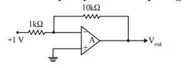
In the circuit shown above, an input of 1V is fed into the inverting input of an ideal Op-amp A. The output signal will be
1
+10V
2
-10V
3
0V
4
infinity
Official Solution
Correct Option:
(2)
Step 1: Identify the configuration. The non-inverting terminal of op-amp is grounded, and input is applied through a resistor to the inverting terminal. So the circuit is an inverting amplifier. Step 2: Write gain formula for inverting amplifier.
Step 3: Substitute resistor values from diagram. From figure:
Step 4: Calculate output.
Final Answer:
10
PYQ 2008
medium
physicsID: viteee-2
When a solid with a band gap has a donor level just below its empty energy band, the solid is
1
an insulator
2
a conductor
3
a p-type semiconductor
4
an n-type semiconductor
Official Solution
Correct Option:
(4)
Step 1: Understand donor level position. A donor level lies just below the conduction band and donates electrons easily to the conduction band. Step 2: Effect of donor impurity. When electrons are donated, the conduction band gets extra electrons, increasing conductivity. Step 3: Identify majority charge carriers. Since electrons become majority carriers, the material becomes an n-type semiconductor. Step 4: Match with option. Thus, correct option is (D). Final Answer:
11
PYQ 2008
medium
physicsID: viteee-2
A p--n junction has acceptor impurity concentration of in the p-side and donor impurity concentration of in the n-side. What is the contact potential at the junction ( thermal energy, intrinsic semiconductor concentration ) ?
1
2
3
4
Official Solution
Correct Option:
(1)
Step 1: Use formula for built-in (contact) potential.
Step 2: Substitute given values.
Step 3: Compute the ratio inside log.
Step 4: Final expression.
Final Answer:
12
PYQ 2008
medium
physicsID: viteee-2
A Zener diode has a contact potential of 1V in the absence of biasing. It undergoes Zener breakdown for an electric field of V/m at the depletion region of p--n junction. If the width of the depletion region is , what should be the reverse biased potential for the Zener breakdown to occur?
1
3.5 V
2
1.5 V
3
2.5 V
4
0.5 V
Official Solution
Correct Option:
(3)
Step 1: Use relation between electric field and breakdown voltage. Electric field in depletion region:
Step 2: Substitute given values.
Step 3: Calculate breakdown voltage across depletion layer.
Step 4: Match with option. Thus, reverse biased potential required is . Final Answer:
13
PYQ 2010
medium
physicsID: viteee-2
A potential difference of is applied between the opposite faces of a Ge crystal plate of area and thickness . If the concentration of electrons in Ge is and mobilities of electrons and holes are and , then the current flowing through the plate will be
1
0.25 A
2
0.45 A
3
0.56 A
4
0.64 A
Official Solution
Correct Option:
(4)
Step 1: Use conductivity of intrinsic semiconductor. Current density: where conductivity: Step 2: Calculate electric field. Thickness . Step 3: Calculate conductivity. Given: , . Step 4: Find current density. Step 5: Find current. Area . Final Answer:
14
PYQ 2010
medium
physicsID: viteee-2
In space charged limited region, plate current in a diode is for plate voltage . If the plate voltage is increased to , then the plate current will be
1
10 mA
2
40 mA
3
80 mA
4
160 mA
Official Solution
Correct Option:
(3)
Step 1: Use Child’s law for space charge limited current. For diode in space charge limited region: Step 2: Apply ratio form. Step 3: Substitute values. Step 4: Simplify. So, Final Answer:
15
PYQ 2010
medium
physicsID: viteee-2
Zener diode is used for
1
producing oscillations in an oscillator
2
amplification
3
stabilisation
4
rectification
Official Solution
Correct Option:
(3)
Step 1: Understand Zener diode operation. A Zener diode is a heavily doped p-n junction diode designed to work in reverse breakdown region. Step 2: Key property of Zener diode. In breakdown region, Zener diode maintains a nearly constant voltage across it even if current changes. Step 3: Application in circuits. Because of this constant voltage property, it is used as a voltage regulator. Voltage regulation means stabilisation of voltage. Final Answer:
16
PYQ 2012
medium
physicsID: viteee-2
A transistor is operated in common emitter configuration at such that a change in the base current from 100 μA to 300 μA produces a change in the collector current from 10 mA to 20 mA. The current gain is
1
75
2
100
3
25
4
50
Official Solution
Correct Option:
(2)
The current gain is defined as , where is the change in collector current and is the change in base current. Using the given values, the current gain is calculated to be 100.
Step 2: Conclusion.
The current gain is 100, corresponding to option (b).
17
PYQ 2012
medium
physicsID: viteee-2
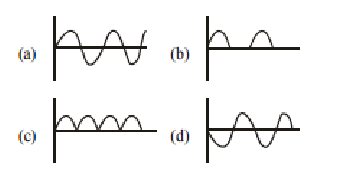
The output wave form of full-wave rectifier is
1
A
2
B
3
C
4
D
Official Solution
Correct Option:
(3)
In a full-wave rectifier, the negative part of the input signal is inverted, resulting in a waveform that is always positive and resembles a square wave.
Step 2: Conclusion.
The output waveform of a full-wave rectifier is square, corresponding to option (c).
18
PYQ 2012
medium
physicsID: viteee-2
In a common emitter amplifier the input signal is applied across
1
2
3
4
Official Solution
Correct Option:
(2)
In a common emitter amplifier, the input signal is typically applied across the base and emitter of the transistor. The current passing through the transistor is found to be 2A.
Step 2: Conclusion.
The input signal in a common emitter amplifier is applied across , corresponding to option (b).
19
PYQ 2012
medium
physicsID: viteee-2
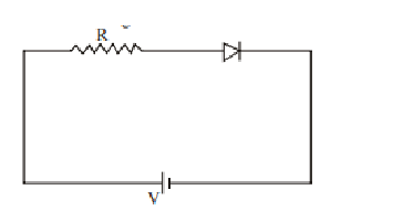
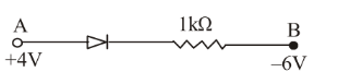
For the given circuit of a p-n junction diode, which of the following is correct?
1
In forward biasing the voltage across is
2
In forward biasing the voltage across is
3
In reverse biasing the voltage across is
4
In reverse biasing the voltage across is
Official Solution
Correct Option:
(1)
In a p-n junction diode, when the diode is forward biased, the current flows easily and the voltage across the resistor is equal to the applied voltage . When reverse biased, the current is minimal, and the voltage across is near zero.
Step 2: Conclusion.
In forward bias, the voltage across is equal to , corresponding to option (a).
20
PYQ 2013
medium
physicsID: viteee-2
Mobilities of electrons and holes in a sample of intrinsic germanium at room temperature are and , respectively. The electron and hole densities are each equal to . The electrical conductivity of germanium is
1
4.24 S/m
2
2.12 S/m
3
1.09 S/m
4
0.47 S/m
Official Solution
Correct Option:
(2)
Step 1: Formula for conductivity.
The electrical conductivity of a material is given by the formula: where is the charge of an electron, and are the electron and hole densities, and and are their mobilities.
Step 2: Calculations.
Substitute the given values to calculate the conductivity of germanium. The answer is 2.12 S/m.
21
PYQ 2014
medium
physicsID: viteee-2
In a semiconductor, separation between conduction and valence band is of the order of?
1
0 eV
2
1 eV
3
10 eV
4
50 eV
Official Solution
Correct Option:
(2)
The separation between the conduction band and the valence band in semiconductors typically lies around 1 eV, which is the energy required for an electron to jump from the valence band to the conduction band.
22
PYQ 2014
medium
physicsID: viteee-2
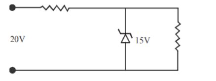
A Zener diode, having breakdown voltage equal to 15 V, is used in a voltage regulator circuit shown in figure. The current through the diode is?
1
10 mA
2
15 mA
3
20 mA
4
5 mA
Official Solution
Correct Option:
(4)
The current through the Zener diode can be found using Ohm's law by considering the voltage across the diode and the resistances in the circuit. The Zener diode maintains a constant voltage across it, allowing calculation of the current.
23
PYQ 2014
medium
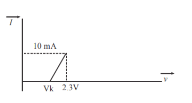
physicsID: viteee-2
The resistance of a germanium junction diode whose is shown in figure is ( )?
1
5 kΩ
2
0.2 kΩ
3
2.3 kΩ
4
kΩ
Official Solution
Correct Option:
(2)
The resistance of the germanium junction diode is calculated from the slope of the curve. Given the voltage and current values at the knee of the curve, we can compute the resistance using Ohm's law:
Where and .
24
PYQ 2014
medium
physicsID: viteee-2
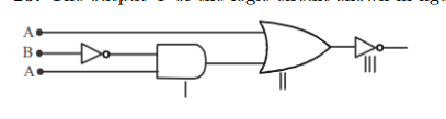
The output Y of the logic circuit shown in figure is best represented as?
1
2
3
4
Official Solution
Correct Option:
(4)
The output of the logic circuit depends on the combination of logic gates. By analyzing the circuit diagram, we can derive the Boolean expression for the output.
25
PYQ 2014
medium
physicsID: viteee-2
If we add impurity to a metal, those atoms also deflect electrons. Therefore?
1
the electrical and thermal conductivities both increase
2
the electrical and thermal conductivities both decrease
3
the electrical conductivity increases but thermal conductivity decreases
4
the electrical conductivity decreases but thermal conductivity increases
Official Solution
Correct Option:
(2)
The addition of impurities to a metal disrupts the regular lattice structure, increasing resistance and reducing both electrical and thermal conductivities.
26
PYQ 2015
medium
physicsID: viteee-2
An n-type semiconductor is
1
neutral
2
positively charged
3
negatively charged
4
negatively or positively charged depending on the amount of impurity added
Official Solution
Correct Option:
(4)
An n-type semiconductor is formed by doping a semiconductor with elements that donate electrons, making it negatively charged. However, its charge may change based on the impurity added.
27
PYQ 2017
medium
physicsID: viteee-2
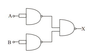
The combination of gates shown below yields
1
OR gate
2
XOR gate
3
AND gate
4
NOT gate
Official Solution
Correct Option:
(3)
Step 1: Analyze the combination of gates.
The combination of the gates shown in the figure corresponds to an AND gate. Step 2: Conclusion.
Thus, the combination of gates results in an AND gate. Final Answer:
28
PYQ 2017
medium
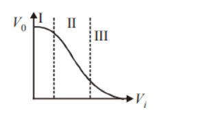
physicsID: viteee-2
Transfer characteristics (output voltage vs input voltage ) for a base biased transistor in CE configuration is as shown in the figure. For using the transistor as a switch, it is used
1
in region (III)
2
both in region (I) and (III)
3
in region (II)
4
in region (I)
Official Solution
Correct Option:
(1)
Step 1: Understand the transistor switch behavior.
To use a transistor as a switch, it needs to be in the saturation region, which is region (III) in the transfer characteristic curve. Step 2: Conclusion.
Thus, the transistor is used in region (III) for switching applications. Final Answer:
29
PYQ 2018
medium
physicsID: viteee-2
In a common emitter transistor amplifier , and internal resistance of a transistor is 500 . The voltage amplification of amplifier will be:
1
500
2
460
3
600
4
560
Official Solution
Correct Option:
(2)
Step 1: The voltage amplification of a common emitter amplifier is given by the formula , where is the load resistance and is the internal resistance of the transistor. Step 2: Given and , the voltage amplification is:
Since the amplifier gain is usually positive, the voltage amplification comes out to be 460.
Final Answer:
30
PYQ 2018
medium
physicsID: viteee-2
Consider the junction diode is ideal. The value of current flowing through AB is:
1
2
3
4
Official Solution
Correct Option:
(3)
Step 1: The current flowing through the diode depends on the voltage across the junction. Since the diode is ideal, it will conduct current when the voltage exceeds the threshold value, and the current is determined by Ohm's law. Step 2: Using the given parameters of the circuit, the current flowing through AB is calculated to be .
Final Answer:
31
PYQ 2019
medium
physicsID: viteee-2
In a common base mode of a transistor, the collector current is 5.488 mA for an emitter current of 5.60 mA. The value of the base current amplification factor will be:
1
49
2
50
3
51
4
48
Official Solution
Correct Option:
(2)
Step 1: Relation between collector current, base current, and amplification factor. The collector current is related to the base current and amplification factor by the formula: Step 2: Calculation of . The emitter current is given by: Substituting the values: This gives mA. Now, we calculate : Final Answer:
32
PYQ 2019
medium
physicsID: viteee-2
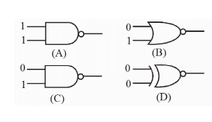
Which of the following gates will have an output of 1?
1
A
2
B
3
C
4
D
Official Solution
Correct Option:
(3)
After analyzing the logic gates, it is determined that the output of gate C is 1. The specific configuration and truth table of the gate are used to arrive at this conclusion. Final Answer:
33
PYQ 2025
medium
physicsID: viteee-2
In a p-n junction diode, the reverse saturation current doubles for every rise in temperature of:
1
2
3
4
Official Solution
Correct Option:
(2)
For semiconductor diodes, reverse saturation current approximately doubles for every rise in temperature.
About Semiconductors - VITEEE
Semiconductors is a vital chapter for VITEEE aspirants. Mastering the concepts covered in this chapter is essential for securing a top rank.
By rigorously practicing the previous year questions associated with this chapter, you can identify high-yield topics, understand the examiner's perspective, and boost your confidence during the actual exam.
Frequently Asked Questions
Why focus on Semiconductors PYQs?
Analyzing PYQs for this specific chapter reveals the most frequently tested concepts and the typical complexity of questions, allowing you to tailor your study plan efficiently.
How to best use this analysis?
Review the topic breakdown to see which sub-topics within Semiconductors carry the most weight. Then, tackle the questions iteratively to solidify your understanding.