The hole and the free electron concentrations in pure silicon at room temperature are given by . When doped with indium, and the hole concentration becomes , the electron concentration is
1
2
3
4
Official Solution
Correct Option: (1)
We use the mass action law:
Given:
So,
02
PYQ 2023
medium
physicsID: ap-eapce
When the temperature of a semiconductor increases then
1
number of free electrons only increases
2
number of holes only increases
3
both number of free electrons and number of holes increase
4
both number of free electrons and number of holes decrease
Official Solution
Correct Option: (3)
In a semiconductor material, the electrical conductivity is significantly lower than that of conductors but higher than that of insulators at room temperature. The conductivity depends on the concentration of charge carriers, which are free electrons and holes. At temperatures above absolute zero, thermal energy can excite electrons from the valence band to the conduction band, creating free electrons in the conduction band and leaving behind holes in the valence band. This process is called thermal generation of electron-hole pairs. When the temperature of a semiconductor increases:
- More thermal energy is available to break covalent bonds in the semiconductor lattice.
- This increased energy causes more electrons to be excited from the valence band to the conduction band.
- As a result, the number of free electrons in the conduction band increases.
- Simultaneously, for every electron that moves to the conduction band, a hole is created in the valence band.
- Therefore, the number of holes in the valence band also increases. The increase in both the number of free electrons and the number of holes leads to an increase in the conductivity of the semiconductor with increasing temperature. Options (A) and (B) are incorrect because the generation of free electrons and holes occurs in pairs due to thermal excitation. Option (D) is incorrect because increasing temperature provides more energy for carrier generation, thus increasing their numbers.
03
PYQ 2024
medium
physicsID: ap-eapce
Pure silicon at 300K has equal electron and hole concentration of m . If the hole concentration increases to m , then the electron concentration in the silicon is:
1
m
2
m
3
m
4
m
Official Solution
Correct Option: (4)
Step 1: Apply Carrier Concentration Formula For intrinsic semiconductors: Step 2: Compute Electron Concentration Thus, the correct answer is m . \bigskip
04
PYQ 2024
medium
physicsID: ap-eapce
A PN junction diode is used as:
1
An amplifier
2
A rectifier
3
An oscillator
4
A modulator
Official Solution
Correct Option: (2)
A PN junction diode is primarily used as a rectifier. It is a semiconductor device that allows current to flow in only one direction, making it ideal for converting alternating current (AC) to direct current (DC). This process of conversion is known as rectification. In the context of the options provided, the correct and commonly accepted use of a PN junction diode is as a rectifier.
05
PYQ 2025
medium
physicsID: ap-eapce
At absolute zero temperature, an intrinsic semiconductor behaves as
1
conductor
2
superconductor
3
insulator
4
semiconductor
Official Solution
Correct Option: (3)
Let’s break this down step by step to determine the behavior of an intrinsic semiconductor at absolute zero and why option (3) is the correct answer. Step 1: Understand the behavior of an intrinsic semiconductor An intrinsic semiconductor is a pure semiconductor without impurities. Its conductivity depends on the excitation of electrons from the valence band to the conduction band, which requires thermal energy to overcome the band gap. Step 2: Analyze the behavior at absolute zero At absolute zero temperature ( ), there is no thermal energy available to excite electrons across the band gap. As a result:
No electrons are in the conduction band.
The valence band is completely filled.
No charge carriers (electrons or holes) are available for conduction.
Therefore, the intrinsic semiconductor behaves as an insulator, as it cannot conduct electricity. Step 3: Confirm the correct answer Since an intrinsic semiconductor has no free charge carriers at absolute zero, it behaves as an insulator, matching option (3). Thus, the correct answer is (3) insulator.
06
PYQ 2025
medium
physicsID: ap-eapce
A transistor works as an amplifier when
1
Emitter-base junction is forward biased and base-collector junction is reverse biased
2
Both emitter-base and base-collector junctions are forward biased
3
Both emitter-base and base-collector junctions are reverse biased
4
Emitter-base junction is reverse biased and base-collector junction is forward biased
Official Solution
Correct Option: (1)
- For a transistor to work as an amplifier, it must operate in the active region.
- In this region, the emitter-base junction is forward biased to allow current injection of charge carriers from emitter to base.
- The base-collector junction is reverse biased so that the charge carriers injected into the base are swept into the collector, resulting in current amplification.
- Other biasing configurations result in cutoff or saturation, not amplification.
07
PYQ 2025
medium
physicsID: ap-eapce
In the given options, the diode that is forward biased is
1
2
3
4
Official Solution
Correct Option: (2)
A diode is forward biased when the anode is at a higher potential than the cathode. In this case, the correct forward bias configuration is +2V → -2V.
08
PYQ 2025
easy
physicsID: ap-eapce
A cc camera is fabricated using a semiconducting material having a band gap of 3 eV. The wavelength of light it can detect is nearly
Official Solution
Correct Option: (1)
09
PYQ 2025
medium
physicsID: ap-eapce
If X, Y and Z are the sizes of the emitter, base and collector of a transistor respectively, then
1
X Z Y
2
X Y Z
3
Z X Y
4
Z Y X
Official Solution
Correct Option: (3)
In a transistor, the collector (Z) is the largest in size, followed by the emitter (X), and the base (Y) is the smallest. This size difference is crucial for the transistor's operation.
10
PYQ 2025
medium
physicsID: ap-eapce
The voltage gain and the current amplification factor of a transistor in common emitter configuration are and respectively. If the collector resistance is , then the base resistance is:
1
2
3
4
Official Solution
Correct Option: (3)
Step 1: Voltage Gain Formula The voltage gain for a transistor in common emitter configuration is: where:
- (current gain),
- (collector resistance),
- . Step 2: Solving for Conclusion Thus, the correct answer is:
11
PYQ 2025
medium
physicsID: ap-eapce
In the given circuit, the input voltage across base resistance 10V. If base-emitter and collector-emitter voltages are zero, then the current amplification factor of the transistor is:
1
25
2
50
3
100
4
125
Official Solution
Correct Option: (3)
Given: , , V, k , k .
Base current A.
Collector current: Since , the collector voltage is the same as the emitter (ground), so A.
Current amplification factor .
12
PYQ 2025
medium
physicsID: ap-eapce
The voltage gain and the current amplification factor of a transistor in common emitter configuration are and respectively. If the collector resistance is , then the base resistance is:
1
2
3
4
Official Solution
Correct Option: (3)
Step 1: Voltage Gain Formula The voltage gain for a transistor in common emitter configuration is: where:
- (current gain),
- (collector resistance),
- . Step 2: Solving for Conclusion Thus, the correct answer is:
13
PYQ 2025
medium
physicsID: ap-eapce
When three NAND logic gates are connected as shown in the figure, then the logic gate equivalent to the circuit is
1
NOT
2
AND
3
OR
4
NOR
Official Solution
Correct Option: (3)
Let's analyze the output of each gate.
NAND gate 1: Inputs are A and A.
Output . (A NAND gate with inputs tied together acts as a NOT gate).
NAND gate 2: Inputs are B and B.
Output . (Acts as a NOT gate).
NAND gate 3: Inputs are X and Y.
Output .
Substitute X and Y:
Using De Morgan's theorem :
Since :
The expression represents the OR logic operation.
Therefore, the equivalent logic gate is OR.
This matches option (3).
14
PYQ 2025
medium
physicsID: ap-eapce
A Zener diode of breakdown voltage 20 V is connected as shown in the given circuit. The current through Zener diode is
1
10 mA
2
4 mA
3
6 mA
4
8 mA
Official Solution
Correct Option: (3)
Step 1: Circuit analysis Supply voltage , Zener voltage . Voltage across resistor: Step 2: Calculate current through resistor Step 3: Current division Current divides through resistor and Zener diode. Current through : Step 4: Current through Zener diode Step 5: Conclusion The current through Zener diode is 6 mA.
15
PYQ 2025
medium
physicsID: ap-eapce
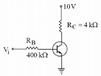
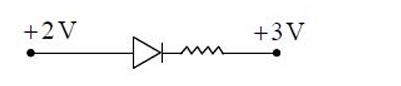
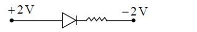
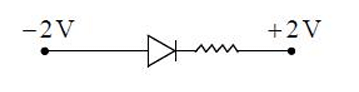
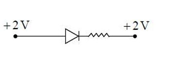
If the junction diodes and in the given circuit are ideal, then the forward biased resistance and reverse biased resistance is infinity:
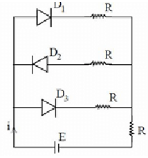
1
2E
2
E
3
4
Official Solution
Correct Option: (4)
In the circuit, and are in parallel with resistors . For ideal diodes: forward resistance = 0, reverse resistance = infinity. If is forward biased (anode at higher potential), it conducts, and is reverse biased (does not conduct). The voltage across (and parallel branch) is . Current through branch: Since has zero resistance, the resistor in series with carries the current. Total current: (since branch does not conduct). Thus, the current is . The answer matches option (4).