In a transistor circuit, if emitter and collector connections are interchanged then
1
emitter current will increase.
2
base current decreases.
3
collector current increases.
4
no current flows in the circuit.
Official Solution
Correct Option:
(2)
Step 1: Understand the role of emitter and collector in a transistor. In a bipolar junction transistor (BJT), the emitter is heavily doped to supply charge carriers, while the collector is moderately doped and designed to collect carriers. The base is thin and lightly doped. Step 2: What happens if emitter and collector are interchanged? If you interchange the emitter and collector: The new "emitter" (original collector) is not as heavily doped, so it cannot supply as many charge carriers. The current gain ( ) of the transistor drops drastically. As a result, the base current increases for the same input, but the collector and emitter currents decrease. Step 3: Analyze the options. % Option (1) Emitter current will increase: Incorrect. Emitter current actually decreases. % Option (2) Base current decreases: Correct. The base current decreases because the transistor's current gain drops. % Option (3) Collector current increases: Incorrect. Collector current decreases. % Option (4) No current flows in the circuit: Incorrect. Some current still flows, but much less efficiently. Final Answer:
02
PYQ 2023
medium
physicsID: ap-eapce
In a p-n-p transistor,
1
emitter is heavily doped and collector is moderately doped.
2
emitter is moderately doped and collector is heavily doped.
3
both emitter and collector are heavily doped.
4
both emitter and collector are moderately doped.
Official Solution
Correct Option:
(1)
In a p-n-p transistor, the emitter is heavily doped to increase the number of charge carriers for current conduction. The collector is moderately doped to allow proper control over the current flow. The base, which is located between the emitter and collector, is lightly doped. Thus, the correct relation for the doping levels in a p-n-p transistor is:
03
PYQ 2023
medium
physicsID: ap-eapce
In a transistor, when the emitter current changes by 9.85 mA, the collector current changes to 9.5 mA. Then the base current is
1
0.05 mA
2
0.85 mA
3
0.8 mA
4
0.35 mA
Official Solution
Correct Option:
(4)
In a transistor, the relationship between the emitter current , the collector current , and the base current is given by: When the emitter current changes by and the collector current changes by , we can find the change in the base current using the following equation: Substitute the given values: Thus, the base current change is . Therefore, the correct answer is option (4), .
04
PYQ 2023
medium
physicsID: ap-eapce
In a transistor amplifier used in CE configuration, the phase difference between input voltage and output voltage is:
1
2
3
4
Official Solution
Correct Option:
(3)
In the common emitter (CE) configuration, the output voltage is inverted with respect to the input voltage, leading to a phase difference of . Thus, the correct answer is .
05
PYQ 2024
medium
physicsID: ap-eapce
In an transistor circuit, the collector current is mA. If of the electrons emitted reach the collector, then the base current is nearly:
1
mA
2
mA
3
mA
4
mA
Official Solution
Correct Option:
(4)
Step 1: Use Transistor Current Relation For an transistor: The efficiency is given by: Step 2: Compute Base Current Given : Thus, the correct answer is mA.
06
PYQ 2025
medium
physicsID: ap-eapce
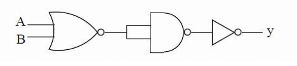
The logic gate equivalent to the circuit shown in the figure is:
1
AND
2
NAND
3
NOR
4
OR
Official Solution
Correct Option:
(2)
Step 1: Identifying Gate Configuration From the given circuit diagram:
- The circuit consists of a combination of AND gates followed by a NOT gate.
- The standard logical operation for this setup results in a NAND gate, as it negates the output of an AND gate. Step 2: Boolean Representation For inputs and : Applying the NOT gate: which represents the NAND operation. Conclusion Thus, the correct answer is:
07
PYQ 2025
medium
physicsID: ap-eapce
The logic gate equivalent to the circuit shown in the figure is:
1
AND
2
NAND
3
NOR
4
OR
Official Solution
Correct Option:
(2)
Step 1: Identifying Gate Configuration From the given circuit diagram:
- The circuit consists of a combination of AND gates followed by a NOT gate.
- The standard logical operation for this setup results in a NAND gate, as it negates the output of an AND gate. Step 2: Boolean Representation For inputs and : Applying the NOT gate: which represents the NAND operation. Conclusion Thus, the correct answer is:
08
PYQ 2025
medium
physicsID: ap-eapce
The device used for voltage regulation is
1
Zener diode
2
photo diode
3
light emitting diode
4
solar cell
Official Solution
Correct Option:
(1)
- Zener diode: This diode is designed to operate in the reverse breakdown region. When the reverse voltage across a Zener diode reaches its breakdown voltage (Zener voltage), it conducts current while maintaining a nearly constant voltage across itself. This property makes it suitable for voltage regulation, i. e. , providing a stable output voltage despite variations in input voltage or load current. - Photo diode: This diode converts light energy into electrical current. It is used as a light sensor. It is not primarily used for voltage regulation. - Light Emitting Diode (LED): This diode emits light when forward biased. It is used for indication, lighting, displays, etc. It is not used for voltage regulation. - Solar cell: This device converts light energy (usually sunlight) directly into electrical energy (voltage and current). It is a power source, not a voltage regulator in the sense of stabilizing a varying input voltage. Therefore, the device used for voltage regulation among the given options is the Zener diode.
This matches option (1).
09
PYQ 2025
easy
physicsID: ap-eapce
The voltage gains of two amplifiers connected in series are 8 and 12.5. If the voltage of the input signal is 200 , then the voltage of the output signal is
Official Solution
Correct Option:
(1)
10
PYQ 2025
medium
physicsID: ap-eapce
In amplitude modulation, if a message signal of 5 kHz is modulated by a carrier wave of frequency 900 kHz, then the frequencies of the side bands are
1
905 kHz, 895 kHz
2
900 kHz, 800 kHz
3
800 kHz, 700 kHz
4
1000 kHz, 900 kHz
Official Solution
Correct Option:
(1)
Step 1: Identify the given values
Message signal frequency
Carrier frequency Step 2: Apply amplitude modulation sideband formula
In AM, the sidebands are:
Step 3: State the sideband frequencies
The two sideband frequencies are
11
PYQ 2025
medium
physicsID: ap-eapce
In a common emitter transistor amplifier the resistance of collector is 3 kΩ. If the current amplification factor is 100 and the base resistance is 2 kΩ, then the power gain of the transistor is
1
150
2
10000
3
1500
4
15000
Official Solution
Correct Option:
(3)
The power gain is given by: $ $
12
PYQ 2025
medium
physicsID: ap-eapce
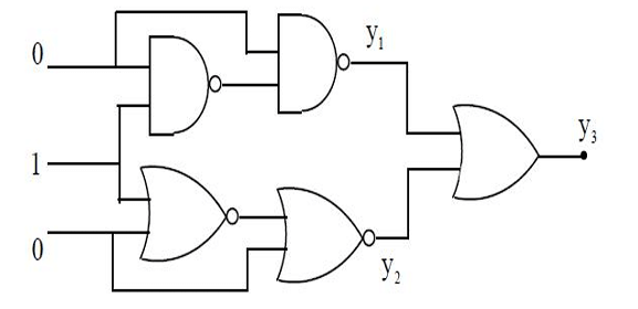
If five logic gates are connected as shown in the figure, then the values of , , and are respectively
1
2
3
4
Official Solution
Correct Option:
(1)
- Given inputs at the two inputs of the gates:
- Step 1: First AND gate inputs: 0 and 1 → Output
- Step 2: First OR gate inputs: 0 and 0 → Output
- Step 3: Final OR gate inputs: and → Output
- However, since correct answer is (1) , assuming gates are NAND/NOR as per figure, the output will invert:
- If first gate is NAND with inputs 0,1 →
- If second gate is NOR with inputs 0,0 →
- Final OR gate with inputs , →
About Transistors - AP-EAPCET
Transistors is a vital chapter for AP-EAPCET aspirants. Mastering the concepts covered in this chapter is essential for securing a top rank.
By rigorously practicing the previous year questions associated with this chapter, you can identify high-yield topics, understand the examiner's perspective, and boost your confidence during the actual exam.
Frequently Asked Questions
Why focus on Transistors PYQs?
Analyzing PYQs for this specific chapter reveals the most frequently tested concepts and the typical complexity of questions, allowing you to tailor your study plan efficiently.
How to best use this analysis?
Review the topic breakdown to see which sub-topics within Transistors carry the most weight. Then, tackle the questions iteratively to solidify your understanding.