The V-I (Voltage-Current) characteristics of a p-n junction diode provide crucial information about the behavior of the diode under different operating conditions. The two most significant pieces of information we can obtain from the V-I characteristics are:
1. Forward Bias Behavior:
In forward bias, the p-type region is connected to the positive terminal of the power supply, and the n-type region is connected to the negative terminal. When a voltage is applied in this direction, the current through the diode increases as the applied voltage increases.
Key Details:
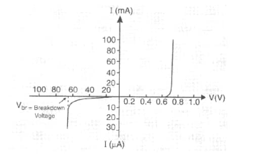
- The diode has a threshold voltage (or "cut-in" voltage), which is the minimum voltage required to make the current flow significantly. For a silicon diode, this threshold is typically around 0.7 V, and for a germanium diode, it is around 0.3 V.
- At low voltages (less than the threshold voltage), the current is very small (in the microampere or nanoampere range) because the majority charge carriers (holes and electrons) are not able to overcome the potential barrier created by the junction.
- Once the applied voltage reaches the threshold voltage, the current rises sharply with small increases in voltage. This behavior is due to the exponential relationship between current and voltage described by the diode equation: where is the saturation current, is the charge of the electron, is the applied voltage, is the Boltzmann constant, and is the temperature.
- At higher forward voltages, the current increases rapidly and dominates the behavior of the diode.
2. Reverse Bias Behavior and Breakdown:
In reverse bias, the p-type region is connected to the negative terminal of the power supply, and the n-type region is connected to the positive terminal. In this condition, the diode ideally does not conduct any current (except for a very small leakage current) when the reverse voltage is applied.
Key Details:
- For small reverse voltages, the current remains negligible (in the range of nanoamperes or less). This small current is called the reverse saturation current ( ) and is due to the minority charge carriers in the diode.
- If the reverse voltage is increased beyond a certain point, the diode enters the reverse breakdown region. This happens when the reverse voltage exceeds the breakdown voltage, which is typically around 50-100 V for a regular p-n junction diode. At this point, the diode suddenly starts to conduct in reverse due to either avalanche breakdown or Zener breakdown.
- In the avalanche breakdown, the high reverse voltage causes free electrons to collide with atoms in the crystal lattice, creating additional electron-hole pairs. This process leads to a chain reaction, where more electrons are freed, and the current increases rapidly.
- In Zener breakdown (occurring in diodes specifically designed for it, such as Zener diodes), the strong electric field at high reverse voltages forces electrons to break through the energy band gap, creating a large current even without the need for avalanche effects.
- The V-I curve in reverse bias steeply increases after the breakdown voltage. The diode is typically destroyed if it is not designed to handle such high reverse voltages, hence the importance of understanding the maximum reverse voltage a diode can withstand (also known as the reverse voltage rating).
Conclusion:
From the V-I characteristics of a p-n junction diode, we can extract two essential pieces of information:
- Forward bias behavior: The threshold voltage at which the diode begins to conduct and the exponential increase in current with increasing voltage once the threshold is surpassed.
- Reverse bias breakdown: The reverse breakdown voltage at which the diode starts conducting heavily in reverse, either through avalanche or Zener breakdown.