CBSE-CLASS-XII SERIES Physics
Semiconductor
19 previous year questions.
Volume: 19 Ques
Yield: Medium
High-Yield Trend
13
2025 6
2024 Chapter Questions 19 MCQs
01
PYQ 2024
easy
physics ID: cbse-cla
Initially, during the formation of a p-n junction:
1
Diffusion current is large and drift current is small.
2
Diffusion current is small and drift current is large.
3
Both the diffusion and the drift currents are large.
4
Both the diffusion and the drift currents are small.
02
PYQ 2024
easy
physics ID: cbse-cla
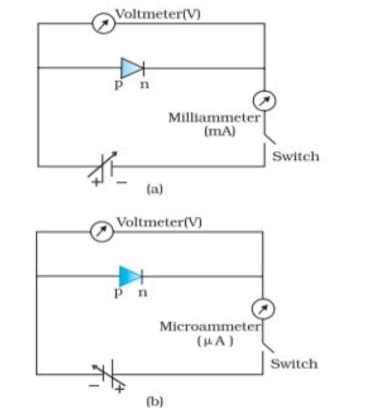
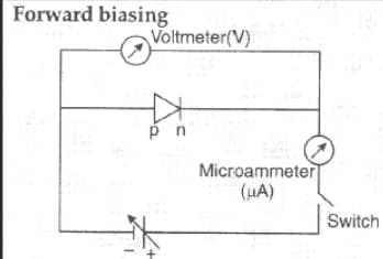
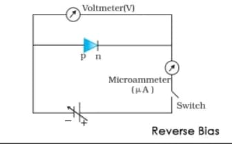
Draw the circuit diagram of a p-n junction diode in
(i) forward biasing and
(ii) reverse biasing.
Also, draw its I-V characteristics in the two cases.
(i) forward biasing and
(ii) reverse biasing.
Also, draw its I-V characteristics in the two cases.
03
PYQ 2024
medium
physics ID: cbse-cla
During the formation of a p-n junction:
1
Electrons diffuse from p-region into n-region and holes diffuse from n-region into p-region.
2
Both electrons and holes diffuse from n-region into p-region.
3
Electrons diffuse from n-region into p-region and holes diffuse from p-region into n-region.
4
Both electrons and holes diffuse from p-region into n-region.
04
PYQ 2024
medium
physics ID: cbse-cla
At a given temperature, the number of intrinsic charge carriers in a semiconductor is cm . It is doped with pentavalent impurity atoms. As a result, the number of holes in it becomes cm . The number of electrons in the semiconductor is:
1
m
2
m
3
m
4
m
05
PYQ 2024
medium
physics ID: cbse-cla
When Ge is doped with a pentavalent impurity, the energy required to free the weakly bound electron from the dopant is about:
1
0.001 eV
2
0.01 eV
3
0.72 eV
4
1.1 eV
06
PYQ 2024
medium
physics ID: cbse-cla
Assertion (A): The temperature coefficient of resistance is positive for metals and negative for p-type semiconductors.
Reason (R): The charge carriers in metals are negatively charged, whereas the majority charge carriers in p-type semiconductors are positively charged.
Reason (R): The charge carriers in metals are negatively charged, whereas the majority charge carriers in p-type semiconductors are positively charged.
1
If both Assertion (A) and Reason (R) are true and Reason (R) is the correct explanation of Assertion (A).
2
If both Assertion (A) and Reason (R) are true and Reason (R) is not the correct explanation of Assertion (A).
3
If Assertion (A) is true and Reason (R) is false.
4
If both Assertion (A) and Reason (R) are false.
07
PYQ 2025
medium
physics ID: cbse-cla
A p-n junction diode is forward biased. As a result,
1
both the potential barrier height and the width of depletion layer decrease.
2
both the potential barrier height and the width of depletion layer increase.
3
the potential barrier height decreases and the width of depletion layer increases.
4
the potential barrier height increases and the width of depletion layer decreases.
08
PYQ 2025
easy
physics ID: cbse-cla
Explain the process of formation of 'depletion layer' and 'potential barrier' in a p-n junction region of a diode, with the help of a suitable diagram. Which feature of junction diode makes it suitable for its use as a rectifier?
09
PYQ 2025
easy
physics ID: cbse-cla
Assertion (A): We cannot form a p-n junction diode by taking a slab of a p-type semiconductor and physically joining it to another slab of an n-type semiconductor.
Reason (R): In a p-type semiconductor while in an n-type semiconductor .
Reason (R): In a p-type semiconductor while in an n-type semiconductor .
1
Both Assertion (A) and Reason (R) are true and Reason (R) is the correct explanation of the Assertion (A).
2
Both Assertion (A) and Reason (R) are true, but Reason (R) is not the correct explanation of the Assertion (A).
3
Assertion (A) is true, but Reason (R) is false.
4
Assertion (A) is false and Reason (R) is also false.
10
PYQ 2025
easy
physics ID: cbse-cla
When a p-n junction diode is forward biased:
1
the barrier height and the depletion layer width both increase.
2
the barrier height increases and the depletion layer width decreases.
3
the barrier height and the depletion layer width both decrease.
4
the barrier height decreases and the depletion layer width increases.
11
PYQ 2025
easy
physics ID: cbse-cla
Explain briefly the formation of diffusion current and drift current in a p-n junction diode.
12
PYQ 2025
hard
physics ID: cbse-cla
Draw circuit arrangement for studying V-I characteristics of a p-n junction diode.
13
PYQ 2025
easy
physics ID: cbse-cla
A p-type Si semiconductor is made by doping an average of one dopant atom per silicon atoms. If the number density of silicon atoms in the specimen is atoms m , find the number of holes created per cubic centimetre in the specimen due to doping. Also give one example of such dopants.
14
PYQ 2025
hard
physics ID: cbse-cla
Germanium crystal is doped at room temperature with a minute quantity of boron. The charge carriers in the doped semiconductor will be:
1
electrons only
2
holes only
3
holes and few electrons
4
electrons and few holes
15
PYQ 2025
medium
physics ID: cbse-cla
In an intrinsic semiconductor, carrier’s concentration is . On doping with impurity atoms, the hole concentration becomes .
[(a)] Identify (i) the type of dopant and (ii) the extrinsic semiconductor so formed.
[(b)] Calculate the electron concentration in the extrinsic semiconductor.
[(a)] Identify (i) the type of dopant and (ii) the extrinsic semiconductor so formed.
[(b)] Calculate the electron concentration in the extrinsic semiconductor.
16
PYQ 2025
easy
physics ID: cbse-cla
What are majority and minority charge carriers of p-type and n-type semiconductors?
17
PYQ 2025
hard
physics ID: cbse-cla
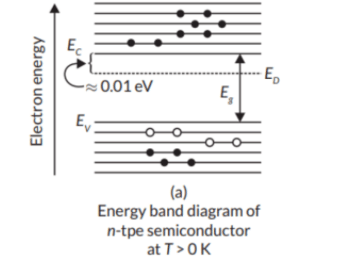
Draw energy band diagrams of n-type and p-type semiconductors at temperature . Show the donor/acceptor energy levels with the order of difference of their energies from the bands.
18
PYQ 2025
easy
physics ID: cbse-cla
Two statements are given, one labelled Assertion (A) and the other labelled Reason (R). Select the correct answer from the codes (A), (B), (C), and (D) as given below.
Assertion (A): n-type semiconductor is not negatively charged.
Reason (R): Neutral pentavalent impurity atom doped in intrinsic semiconductor (neutral) donates its fifth unpaired electron to the crystal lattice and becomes a positive donor.
Assertion (A): n-type semiconductor is not negatively charged.
Reason (R): Neutral pentavalent impurity atom doped in intrinsic semiconductor (neutral) donates its fifth unpaired electron to the crystal lattice and becomes a positive donor.
1
Both Assertion (A) and Reason (R) are true and Reason (R) is the correct explanation of the Assertion (A).
2
Both Assertion (A) and Reason (R) are true, but Reason (R) is not the correct explanation of the Assertion (A).
3
Assertion (A) is true, but Reason (R) is false.
4
Both Assertion (A) and Reason (R) are false.
19
PYQ 2025
medium
physics ID: cbse-cla
When a p-n junction diode is forward biased:
1
The barrier height and the depletion layer width both increase.
2
The barrier height increases and the depletion layer width decreases.
3
The barrier height and the depletion layer width both decrease.
4
The barrier height decreases and the depletion layer width increases.
About Semiconductor - CBSE-CLASS-XII
Semiconductor is a vital chapter for CBSE-CLASS-XII aspirants. Mastering the concepts covered in this chapter is essential for securing a top rank.
By rigorously practicing the previous year questions associated with this chapter, you can identify high-yield topics, understand the examiner's perspective, and boost your confidence during the actual exam.
Frequently Asked Questions
Why focus on Semiconductor PYQs?
Analyzing PYQs for this specific chapter reveals the most frequently tested concepts and the typical complexity of questions, allowing you to tailor your study plan efficiently.
How to best use this analysis?
Review the topic breakdown to see which sub-topics within Semiconductor carry the most weight. Then, tackle the questions iteratively to solidify your understanding.