Semiconductor Electronics Materials Devices And Simple Circuits
25 previous year questions.
High-Yield Trend
Chapter Questions 25 MCQs
Assertion : In a semiconductor diode, the thickness of the depletion layer is not fixed.
Reason (R): Thickness of depletion layer in a semiconductor device depends upon many factors such as biasing of the semiconductor.
Assertion (A): A hole is an apparent free particle with effective positive electronic charge.
Reason (R): A hole is not necessarily a vacancy left behind by an electron in the valence band.
The graph shows the variation of current with voltage for a p-n junction diode. Estimate the dynamic resistance of the diode at V.
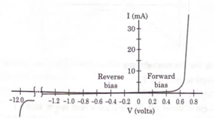
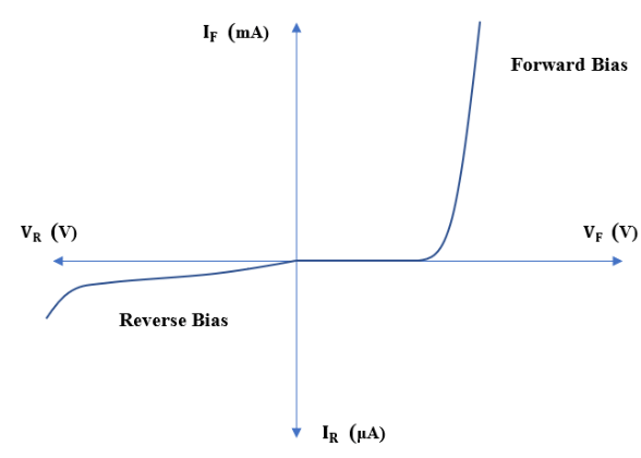
(b) Show the shape of the characteristics of a diode.
(c) Mention two information that you can get from these characteristics.
Assertion (A): We cannot form a p-n junction diode by taking a slab of a p-type semiconductor and physically joining it to another slab of an n-type semiconductor.
Reason (R): In a p-type semiconductor, while in an n-type semiconductor .
About Semiconductor Electronics Materials Devices And Simple Circuits - CBSE-CLASS-XII
Semiconductor Electronics Materials Devices And Simple Circuits is a vital chapter for CBSE-CLASS-XII aspirants. Mastering the concepts covered in this chapter is essential for securing a top rank.
By rigorously practicing the previous year questions associated with this chapter, you can identify high-yield topics, understand the examiner's perspective, and boost your confidence during the actual exam.
Frequently Asked Questions
Why focus on Semiconductor Electronics Materials Devices And Simple Circuits PYQs?
Analyzing PYQs for this specific chapter reveals the most frequently tested concepts and the typical complexity of questions, allowing you to tailor your study plan efficiently.
How to best use this analysis?
Review the topic breakdown to see which sub-topics within Semiconductor Electronics Materials Devices And Simple Circuits carry the most weight. Then, tackle the questions iteratively to solidify your understanding.