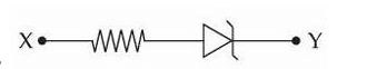
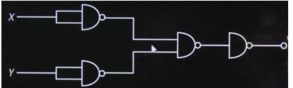
In the following logic circuit the sequence of the inputs A, B are (0, 0), (0, 1), (1, 0) and (1, 1). The output Y for this sequence will be :
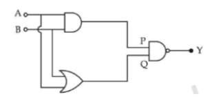
1
1, 1, 1, 0
2
1, 0, 1, 0
3
0, 1, 0, 1
4
0, 0, 1, 1
Official Solution
Correct Option: (1)
Step 1: Understanding the Concept: The circuit consists of three logic gates. The first gate (top) is an AND gate with inputs and . The second gate (bottom) is an OR gate with inputs and . The third gate (right) is a NAND gate that takes the outputs of the first two gates as its inputs. Step 2: Key Formula or Approach: Let be the output of the AND gate: . Let be the output of the OR gate: . The final output is the NAND of and :
Step 3: Detailed Explanation: Let's evaluate the output for each input pair: 1. For : , . Output . 2. For : , . Output . 3. For : , . Output . 4. For : , . Output . The resulting sequence of outputs is 1, 1, 1, 0. Step 4: Final Answer: The sequence for the given inputs is 1, 1, 1, 0.
02
PYQ 2026
medium
physicsID: jee-main
For the given circuit (shown in part A) the time dependent input voltage and corresponding output are shown in parts (B) and (C), respectively. Identify the components that are used in the circuit between and .}
1
2
3
4
Official Solution
Correct Option: (2)
Concept: The circuit in part (A) contains:
An ideal diode
A Zener diode with breakdown voltage V
The output waveform shows clipping at: Thus the circuit behaves like a bidirectional voltage limiter. Step 1:Analyze positive half cycle} During positive input:
Zener diode reaches breakdown at V.
Output voltage is limited to V.
Step 2:Analyze negative half cycle} During negative input:
The other diode conducts normally.
Voltage is limited to V.
Step 3:Equivalent circuit} Such symmetrical clipping occurs when two diodes are connected in opposite directions between and . Thus the correct option corresponds to:
03
PYQ 2026
easy
physicsID: jee-main
What is the equivalent gate for the following digital circuit?
1
AND gate
2
OR gate
3
NAND gate
4
NOR gate
Official Solution
Correct Option: (2)
Concept: Use properties of universal gates and De Morgan's theorem: Also note that a NAND gate with both inputs same acts as a NOT gate. Step 1: Analyze the first stage.} Each input passes through a NAND gate whose inputs are tied together. Thus, So outputs of first stage are: Step 2: Second stage NAND operation.} These inputs go to a NAND gate: Using De Morgan's theorem: Step 3: Final gate.} The last gate is again a NAND with both inputs tied together, which acts as a NOT gate: Thus the final output becomes: which is the function of an OR gate.