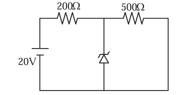
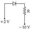
A Zener diode of breakdown voltage 10V is used as a voltage regulator as shown in the figure. The current through the Zener diode is
1
50 mA
2
0
3
30 mA
4
20 mA
Official Solution
Correct Option:
(3)
The problem asks for the current flowing through the Zener diode in the given voltage regulator circuit.
Concept Used:
The circuit is a Zener diode voltage regulator. When a Zener diode is reverse-biased and the voltage across it is greater than or equal to its breakdown voltage ( ), it enters the breakdown region and maintains a nearly constant voltage across its terminals, equal to . The current in the circuit is then analyzed using Ohm's law and Kirchhoff's Current Law (KCL).
The steps to solve this are:
Verify that the Zener diode is operating in its breakdown region.
Once confirmed, the voltage across the load resistor is fixed at the Zener voltage, .
Calculate the total current flowing from the source through the series resistor.
Calculate the current flowing through the load resistor.
Apply KCL at the junction to find the current flowing through the Zener diode.
Step-by-Step Solution:
Step 1: Confirm that the Zener diode is in breakdown mode.
For the diode to be in breakdown, the voltage across it must be at least . If we assume for a moment that the Zener diode is not present, the voltage across the resistor (the open-circuit voltage ) would be given by the voltage divider rule:
Since is greater than the Zener breakdown voltage , the Zener diode is operating in its breakdown region. Therefore, it will regulate the voltage across the parallel branch to .
Step 2: Calculate the total current ( ) flowing from the source.
Since the voltage across the Zener diode (and the parallel resistor) is fixed at , the voltage drop across the series resistor ( ) is:
The total current flowing from the source is the current through this series resistor, which can be found using Ohm's law:
Step 3: Calculate the current ( ) through the load resistor.
The voltage across the load resistor ( ) is the Zener voltage, . The current through the load is:
Step 4: Apply Kirchhoff's Current Law (KCL) to find the Zener current ( ).
The total current from the source splits into two paths: one through the Zener diode ( ) and one through the load resistor ( ). According to KCL:
Solving for the Zener current:
Final Computation & Result:
Substitute the calculated values for the total current and load current:
The current through the Zener diode is 30 mA.
02
PYQ 2024
medium
physicsID: jee-main
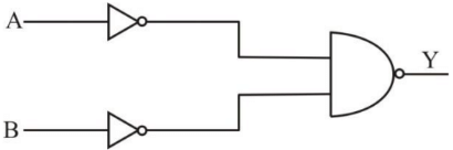
Identify the logic operation performed by the given circuit.
1
NAND
2
NOR
3
OR
4
AND
Official Solution
Correct Option:
(3)
The given circuit consists of two NOT gates and one OR gate. To identify the logic operation, let's analyze the circuit step-by-step:
Each input (A and B) passes through a NOT gate. The function of a NOT gate is to invert the input signal.
If A = 0, then after NOT, the output is 1.
If B = 0, then after NOT, the output is 1.
If A = 1, then after NOT, the output is 0.
If B = 1, then after NOT, the output is 0.
The outputs of the NOT gates are then fed into an OR gate. The OR gate outputs 1 if at least one of its inputs is 1.
For (A', B') = (0, 0), the OR gate output is 0.
For (A', B') = (0, 1) or (1, 0) or (1, 1), the OR gate output is 1.
Combining these, we realize that the entire circuit performs an OR operation on the outputs of the NOT gates. Since the NOT gates invert A and B before passing to the OR gate, the final operation resembles an OR operation.
Therefore, the correct answer is OR.
03
PYQ 2024
medium
physicsID: jee-main
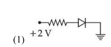
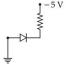
Which of the following circuits is reverse-biased?
1
2
3
4
Official Solution
Correct Option:
(4)
To determine which of the circuits is reverse-biased, we need to understand what reverse biasing means in the context of a diode within a circuit.
A diode is said to be reverse-biased when the voltage at the cathode (negative side) is higher than the voltage at the anode (positive side). This prevents the current from flowing through the diode.
In contrast, a diode is forward-biased when the voltage at the anode is higher than at the cathode, allowing current to flow.
From the analysis, Circuit 4 is the only circuit where the diode is reverse-biased. Hence, the correct answer is:
This solution is based on the fundamental principles of diode operation concerning forward and reverse biasing. In a reverse-biased condition, current does not flow due to the orientation of the voltage across the diode.
04
PYQ 2026
medium
physicsID: jee-main
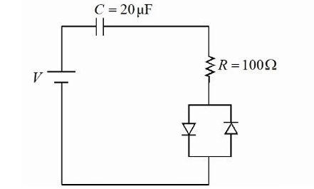
Consider a circuit consisting of a capacitor (20 μF), resistor and two identical diodes as shown in figure. The resistance of diode under forward biasing condition is 10 Ω. The time constant of the circuit is s. The value of is ________.
1
2.2
2
2.0
3
2.1
4
2.4
Official Solution
Correct Option:
(1)
Step 1: Understanding the Concept:
The time constant ( ) of an RC circuit is given by . In a circuit with diodes, the net resistance depends on the direction of current flow. If the capacitor is charging or discharging through a specific path, only the forward-biased diode contributes its resistance.
Step 2: Key Formula or Approach:
1.
2. In forward bias, .
3. Total resistance (assuming they are in series in the active branch).
Step 3: Detailed Explanation:
1. Identifying the active branch: Usually, in such problems, the capacitor discharges through the resistor and one forward-biased diode.
2. .
3. .
4. .
5. Comparing with , we find .
Step 4: Final Answer:
The value of is 2.2.
05
PYQ 2026
medium
physicsID: jee-main
In a semiconductor p-n diode, the doping concentrations on p-side and n-side are and , respectively. Which one of the following statements is true?
1
Widths of depletion region on either side of the interface are equal
2
The depletion region width is more on p-side compared to that in n-side
3
The depletion region width is more on n-side compared to that in p-side
4
No depletion region forms because of unequal doping concentrations
Official Solution
Correct Option:
(2)
Step 1: Understanding the Concept:
In a p-n junction, the depletion region must satisfy the condition of charge neutrality. This means the total ionized charge on the p-side must equal the total ionized charge on the n-side. : Key Formula or Approach:
Charge neutrality condition: .
Where are acceptor/donor concentrations and are widths of depletion layers on each side. Step 2: Detailed Explanation:
Given:
.
.
From neutrality: .
.
Since , the depletion region extends much further into the p-side.
This is a general principle: the depletion region is always wider on the more lightly doped side. Step 3: Final Answer:
The depletion region width is more on the p-side compared to that in the n-side.
06
PYQ 2026
medium
physicsID: jee-main
Given below are two statements: one is labelled as Assertion A and the other is labelled as Reason R
Assertion A: A diode under reverse-biased condition provides very small current which is nearly independent of voltage until a critical limit at which the current increases drastically.
Reason R: Below the critical voltage limit, only majority charge carriers flow which increases drastically above critical voltage.
choose the correct answer from the options given below:
1
Both A and R are true and R is the correct explanation of A
2
Both A and R are true but R is NOT the correct explanation of A
3
A is true but R is false
4
A is false but R is true
Official Solution
Correct Option:
(3)
Step 1: Understanding the Concept:
In a p-n junction diode, reverse bias occurs when the n-region is connected to a higher potential than the p-region. This increases the barrier height, preventing majority carrier flow but allowing a small number of minority carriers to cross.
Step 2: Key Formula or Approach:
The reverse current consists of a reverse saturation current due to minority carriers. At a high enough reverse voltage (Breakdown voltage), the current increases sharply due to Zener or Avalanche breakdown.
Step 3: Detailed Explanation:
Assertion A is correct: In reverse bias, a very small "reverse saturation current" flows, which is nearly constant until the breakdown voltage is reached. At breakdown, the current increases drastically.
Reason R is incorrect: Below the breakdown limit, the current is due to minority charge carriers, not majority carriers. Majority carriers are pushed away from the junction in reverse bias. Above the critical voltage, current increases due to carrier multiplication or tunneling, but the statement about majority carriers flowing below the limit is fundamentally wrong.
Step 4: Final Answer:
Assertion A is true, but Reason R is false.
About Electronic Devices - JEE-MAIN
Electronic Devices is a vital chapter for JEE-MAIN aspirants. Mastering the concepts covered in this chapter is essential for securing a top rank.
By rigorously practicing the previous year questions associated with this chapter, you can identify high-yield topics, understand the examiner's perspective, and boost your confidence during the actual exam.
Frequently Asked Questions
Why focus on Electronic Devices PYQs?
Analyzing PYQs for this specific chapter reveals the most frequently tested concepts and the typical complexity of questions, allowing you to tailor your study plan efficiently.
How to best use this analysis?
Review the topic breakdown to see which sub-topics within Electronic Devices carry the most weight. Then, tackle the questions iteratively to solidify your understanding.