Logic Gates
40 previous year questions.
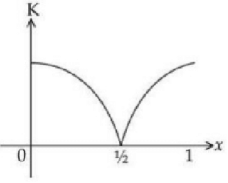
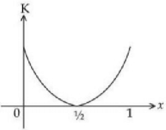
High-Yield Trend
Chapter Questions 40 MCQs
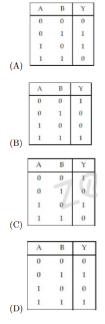
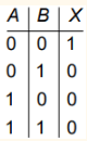
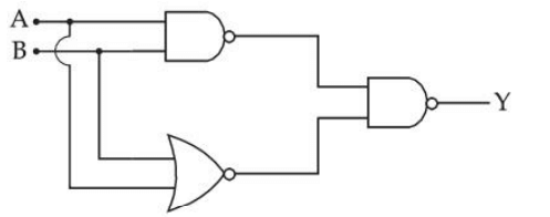
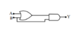
The truth table for the following logic circuit is: 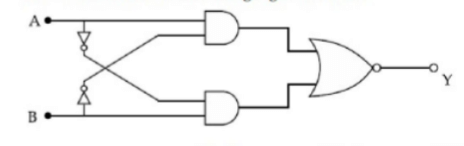
A
B
C
D
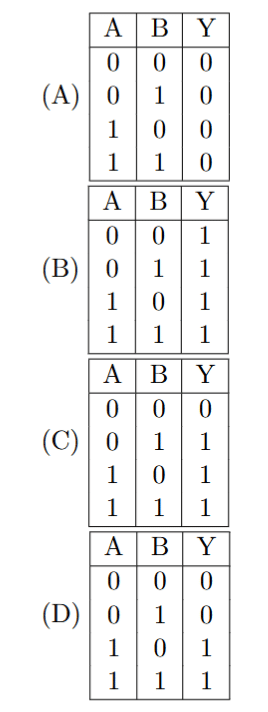
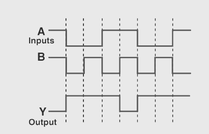
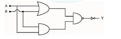
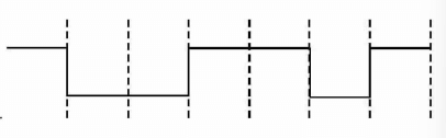
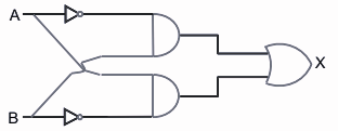
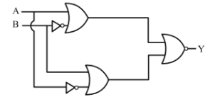
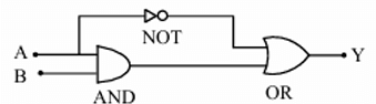
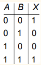
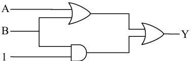
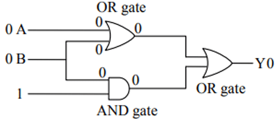
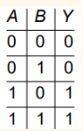
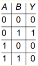
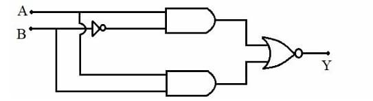
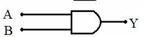
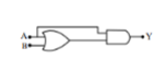
Find the truth table for the function Y of A and B represented in the following figure. 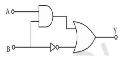
A
B
C
D
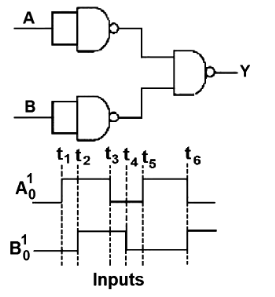
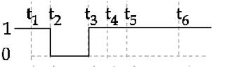
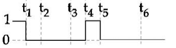
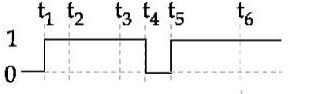
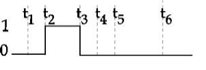
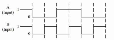
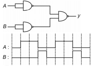
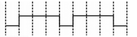
A logic gate circuit has two inputs A and B and output Y. The voltage waveforms of A, B and Y are shown below.
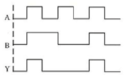
The logic gate circuit is :


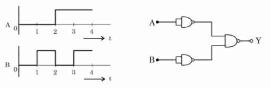
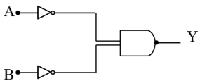
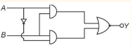
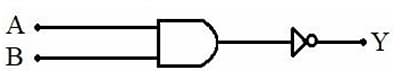
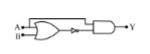
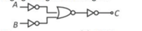
Which logic gate is specified by given circuit


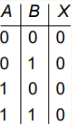
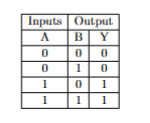
| A | B | X |
|---|---|---|
0 0 1 1 | 0 1 0 1 | 1 0 0 0 |
| A | B | X |
|---|---|---|
0 0 1 1 | 0 1 0 1 | 0 1 1 1 |
| A | B | X |
|---|---|---|
0 0 1 1 | 0 1 0 1 | 0 1 1 0 |
| A | B | X |
|---|---|---|
0 0 1 1 | 0 1 0 1 | 1 0 1 0 |
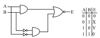
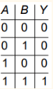
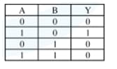
In the truth table of the above circuit the value of X and Y are
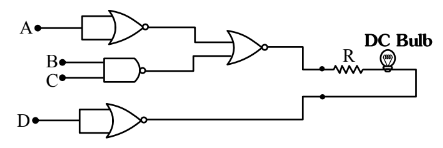
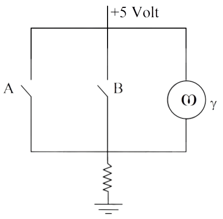
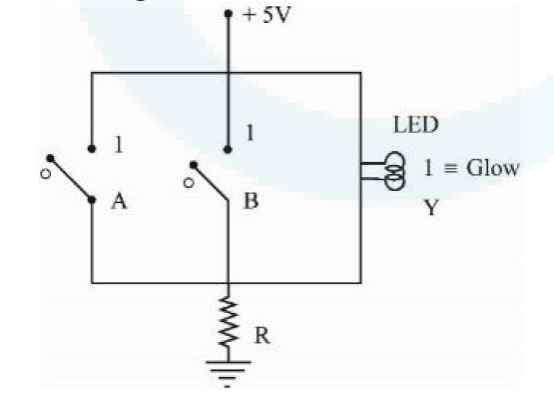
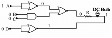
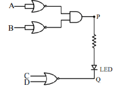
For which of the following combination, bulb will glow (ON):
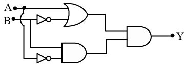
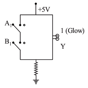
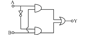
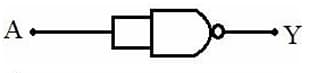
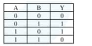
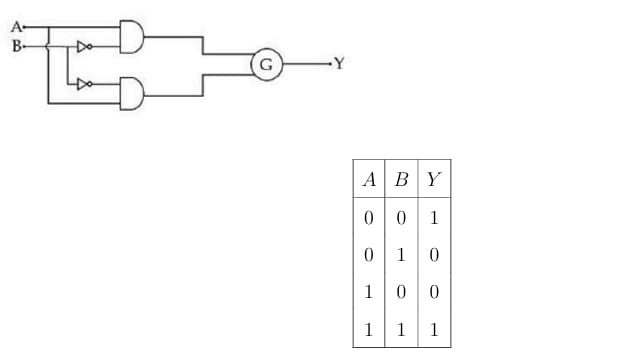
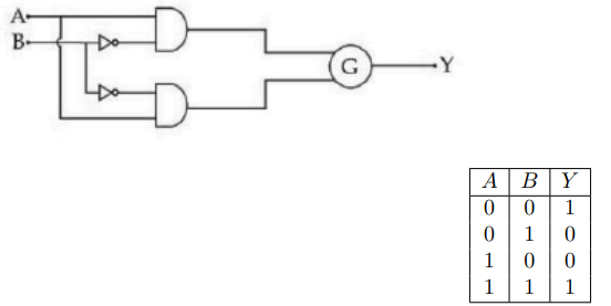
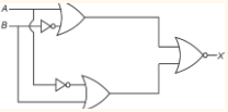 Draw truth table of given gate circuit.
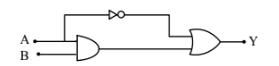
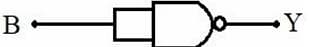
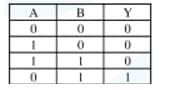
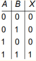
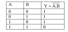
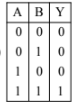
| A | B | Y |
| 0 | 0 | 1 |
| 0 | 1 | 1 |
| 1 | 0 | 1 |
| 1 | 1 | 0 |
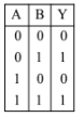
| A | B | Y |
| 0 | 0 | 0 |
| 0 | 1 | 1 |
| 1 | 0 | 0 |
| 1 | 1 | 1 |
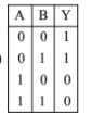
| A | B | Y |
| 0 | 0 | 0 |
| 0 | 1 | 0 |
| 1 | 0 | 0 |
| 1 | 1 | 1 |
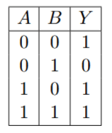
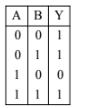
| A | B | Y |
| 0 | 0 | 1 |
| 0 | 1 | 0 |
| 1 | 0 | 1 |
| 1 | 1 | 0 |

For the circuit shown above, the equivalent gate is:
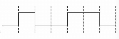
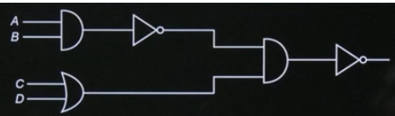
Which of the following circuits has the same output as that of the given circuit?

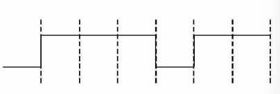
Which of the following circuits has the same output as that of the given circuit?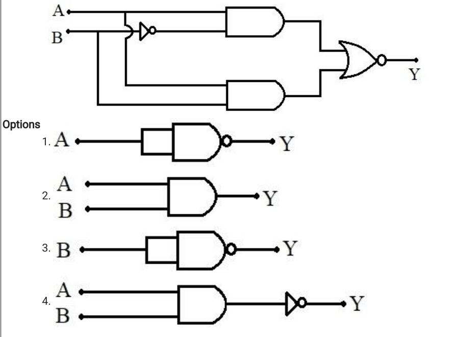
A
B
C
D
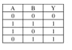
To obtain the given truth table, the following logic gate should be placed at G:

Consider the following logic circuit.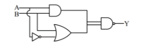
The output is Y = 0 when :
About Logic Gates - JEE-MAIN
Logic Gates is a vital chapter for JEE-MAIN aspirants. Mastering the concepts covered in this chapter is essential for securing a top rank.
By rigorously practicing the previous year questions associated with this chapter, you can identify high-yield topics, understand the examiner's perspective, and boost your confidence during the actual exam.
Frequently Asked Questions
Why focus on Logic Gates PYQs?
Analyzing PYQs for this specific chapter reveals the most frequently tested concepts and the typical complexity of questions, allowing you to tailor your study plan efficiently.
How to best use this analysis?
Review the topic breakdown to see which sub-topics within Logic Gates carry the most weight. Then, tackle the questions iteratively to solidify your understanding.