Semiconductor Electronics Materials Devices And Simple Circuits
78 previous year questions.
High-Yield Trend
Chapter Questions 78 MCQs
Statement II : The n-type semiconductor has net negative charge.
In the light of the above statements, choose the most appropriate answer from the options given below :
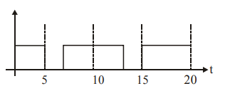
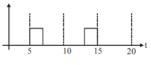
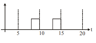
Choose the correct waveform that can represent the voltage across R of the following circuit, assuming the diode is ideal one : 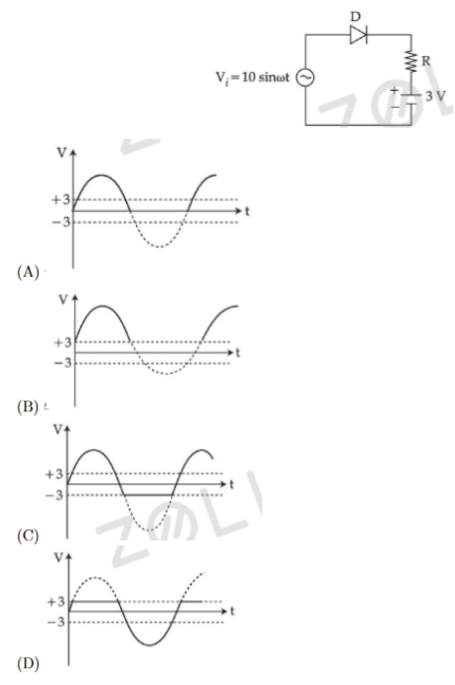
A zener diode of power rating 2 W is to be used as a voltage regulator. If the zener diode has a breakdown of 10 V and it has to regulate voltage fluctuated between 6 V and 14 V, the value of R for safe operation should be _________ . 
A circuit is arranged as shown in figure. The output voltage is equal to ________ V. 
For the given circuit, the power across zener diode is __________ mW. 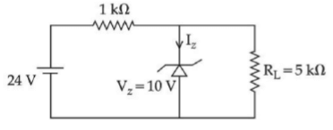
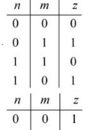
Four NOR gates are connected as shown in figure. The truth table for the given figure is : 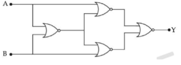
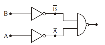
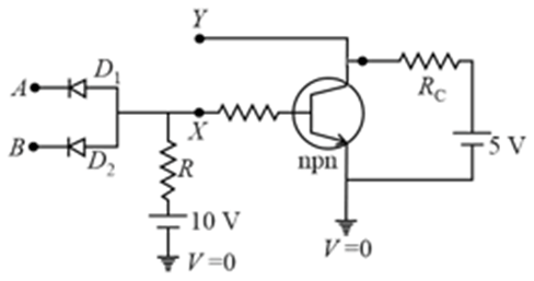
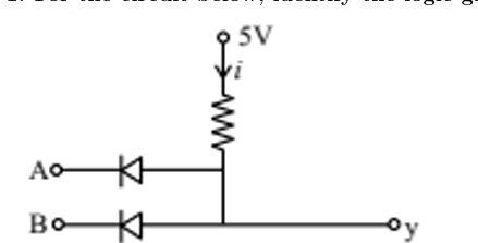
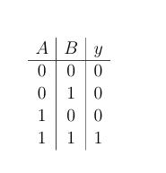
Identify the logic operation carried out by the given circuit : 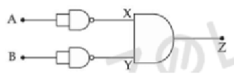
Match List I with List II. 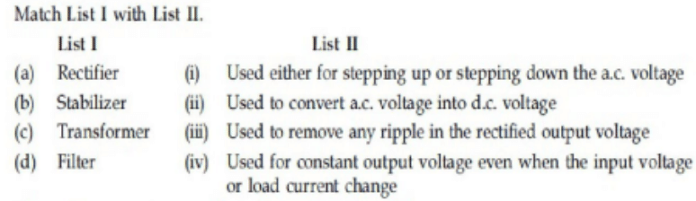
Choose the correct answer from the options given below:
\begin{center} \includegraphics[width=0.5\textwidth]{logic_gates} \end{center}
Statement II : To get a steady dc output from the pulsating voltage received from a full wave rectifier we can connect an inductor in series with .
In the light of the above statements, choose the most appropriate answer from the options given below :
Identify the logic operation carried out. 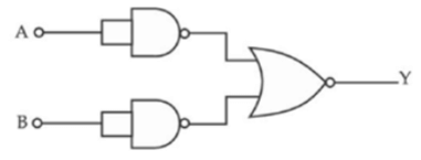
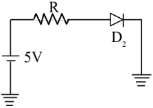
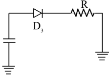
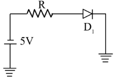
A 5V battery is connected across the points X and Y. Assume D1 and D2 to be normal silicon diodes. Find the current supplied by the battery if the +ve terminal of the battery is connected to point X and -ve to point Y. 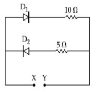
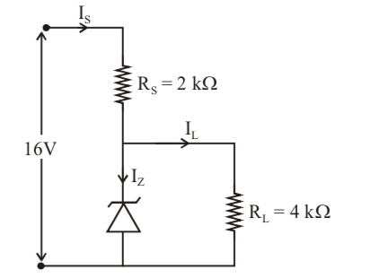
In connection with the circuit drawn below (assuming a Zener diode circuit with , , , ), the value of current flowing through 2 kΩ resistor is _________ × 10⁻⁴ A. 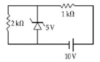
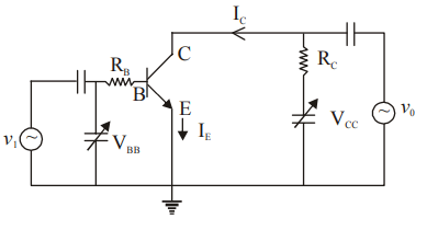
The typical output characteristics curve for a transistor working in the common-emitter configuration is shown in the figure. The estimated current gain from the figure is ________. 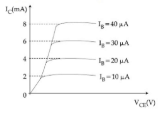
Given below are two statements: One is labelled as Assertion A and the other is labelled as Reason R.
Assertion A :n-p-n transistor permits more current than a p-n-p transistor.
Reason R: Electrons have greater mobility as a charge carrier.
Choose the correct answer from the options given below:
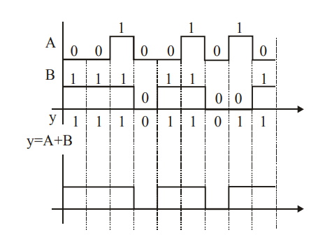
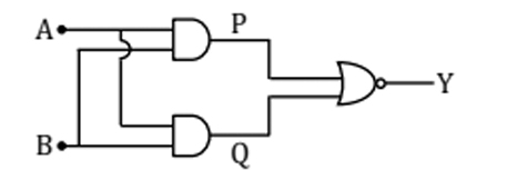
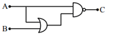
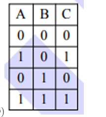
In the following circuit, the correct relation between output (Y) and inputs A and B will be:
Two long parallel conductors and are separated by a distance cm and carrying currents of A and A respectively. The conductors are placed along x-axis in X–Y plane. There is a point P located between the conductors (as shown in figure). A charge particle of coulomb is passing through the point P with velocity m/s; where and represents unit vector along x & y axis respectively. The force acting on the charge particle is . The value of x is: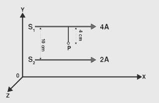
A potential barrier of 0.4 V exists across a p-n junction. An electron enters the junction from the n-side with a speed of 6.0 × 10⁵ ms–1. The speed with which electrons enters the p side will be
ms-1
the value of x is _________.
(Give mass of electron = 9 × 10–31 kg, charge on electron = 1.6 × 10⁻¹⁹ C)
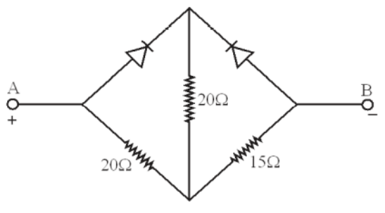
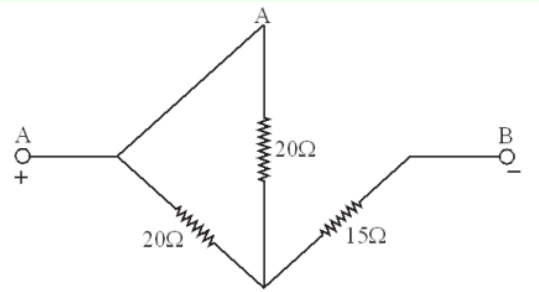
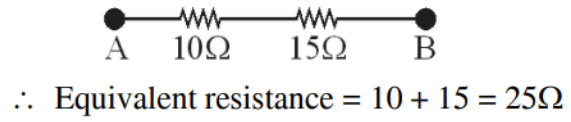
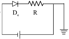
Two ideal diodes are connected in the network as shown in figure The equivalent resistance between and is ______
The effect of increase in temperature on the number of electrons in conduction band and resistance of a semiconductor will be as:
Statement II: When such P-type and N-type semi-conductors, are fused to make a junction, a current will automatically flow which can be detected with an externally connected ammeter.
In the light of above statements, choose the most appropriate answer from the options given below
Assertion A: Photodiodes are preferably operated in reverse bias condition for light intensity measurement
Reason R: The current in the forward bias is more than the current in the reverse bias for a junction diode
In the light of the above statements, choose the correct answer from the options given below:
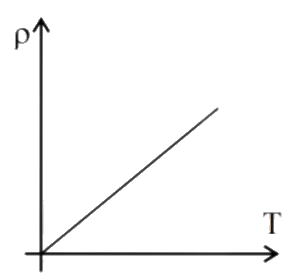
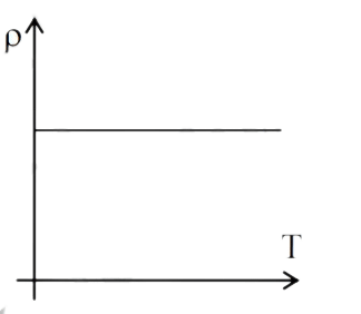
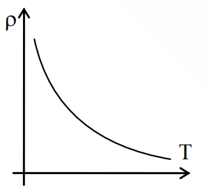
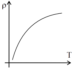
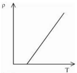
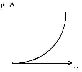
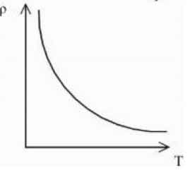
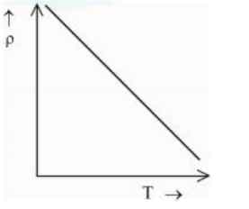
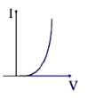
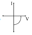
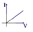
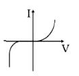
Choose correct graph of resistivity and temperature for semi-conductor material.
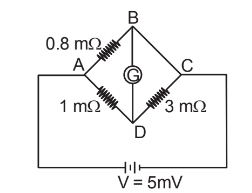
Sliding contact of a potentiometer is in the middle of the potentiometer wire having resistance as shown in the figure. An external resistance of is connected via the sliding contact.
The current is : 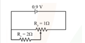
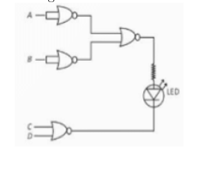
The given circuit works as: 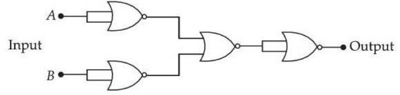
Assuming in forward bias condition there is a voltage drop of V across a silicon diode, the current through diode in the circuit shown is ________ mA. (Assume all diodes in the given circuit are identical) 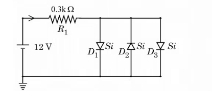
A. the maximum wavelength of the radiation of Lyman series is 4/3R
B. the Balmer series lies in the visible region of the spectrum
C. the minimum wavelength of the radiation of Paschen series is 9/R
D. the minimum wavelength of Lyman series is 5/4R
Choose the correct answer from the options given below :
Three silicon diodes connected parallel to each other as shown. Forward voltage of diode is 0.7 V. Find current through diode A : 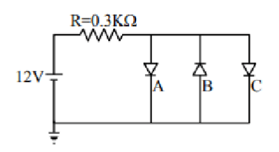
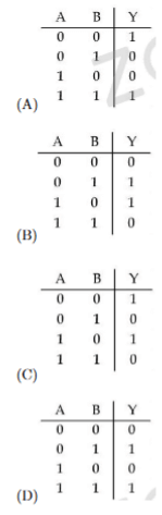
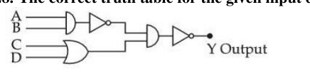
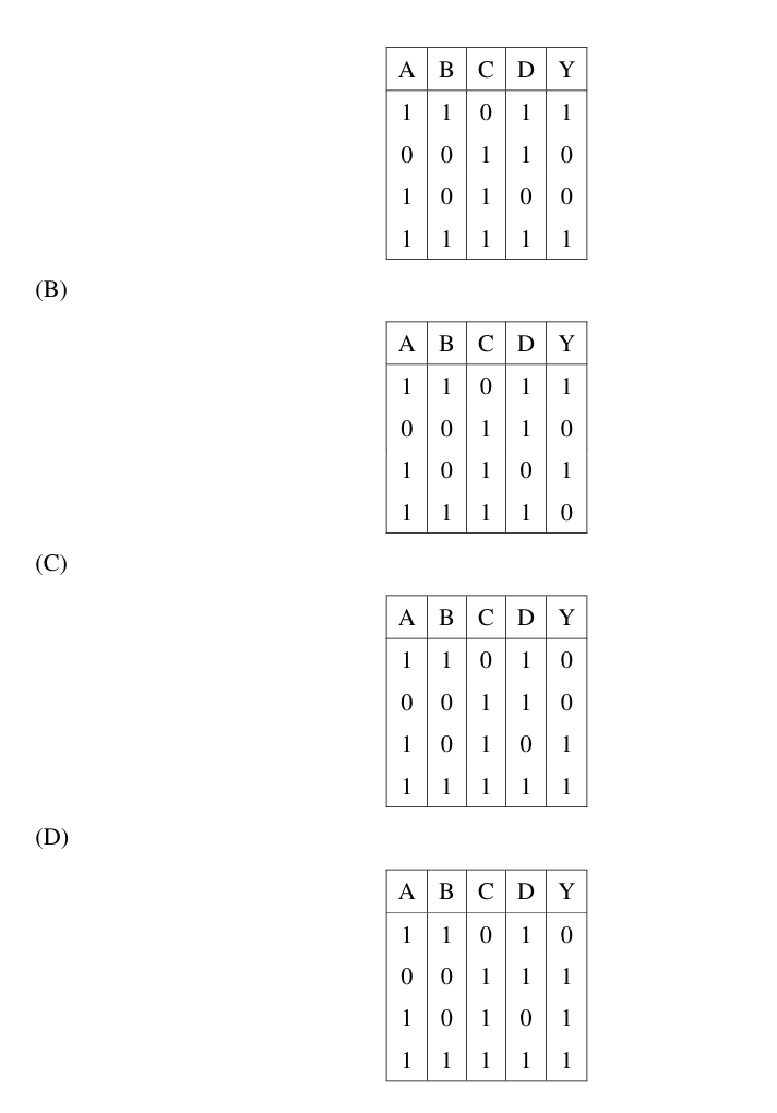
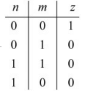
For the given logic gate circuit, which of the following is the correct truth table ? 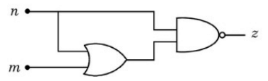


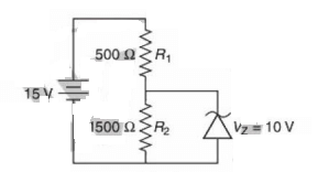
In the given circuit diagram, mA and the Zener voltage is V. If , find the value of (in ). 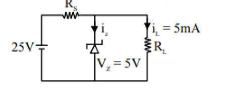
The correct structure of is
About Semiconductor Electronics Materials Devices And Simple Circuits - JEE-MAIN
Semiconductor Electronics Materials Devices And Simple Circuits is a vital chapter for JEE-MAIN aspirants. Mastering the concepts covered in this chapter is essential for securing a top rank.
By rigorously practicing the previous year questions associated with this chapter, you can identify high-yield topics, understand the examiner's perspective, and boost your confidence during the actual exam.
Frequently Asked Questions
Why focus on Semiconductor Electronics Materials Devices And Simple Circuits PYQs?
Analyzing PYQs for this specific chapter reveals the most frequently tested concepts and the typical complexity of questions, allowing you to tailor your study plan efficiently.
How to best use this analysis?
Review the topic breakdown to see which sub-topics within Semiconductor Electronics Materials Devices And Simple Circuits carry the most weight. Then, tackle the questions iteratively to solidify your understanding.